Display device and its manufacturing method
A technology for a display device and a manufacturing method, which is applied to static indicators, instruments, nonlinear optics, etc., can solve problems such as poor display, leakage short circuit, and poor open circuit, and achieve the effects of reducing poor display and preventing voltage drop
- Summary
- Abstract
- Description
- Claims
- Application Information
AI Technical Summary
Problems solved by technology
Method used
Image
Examples
Embodiment approach 1
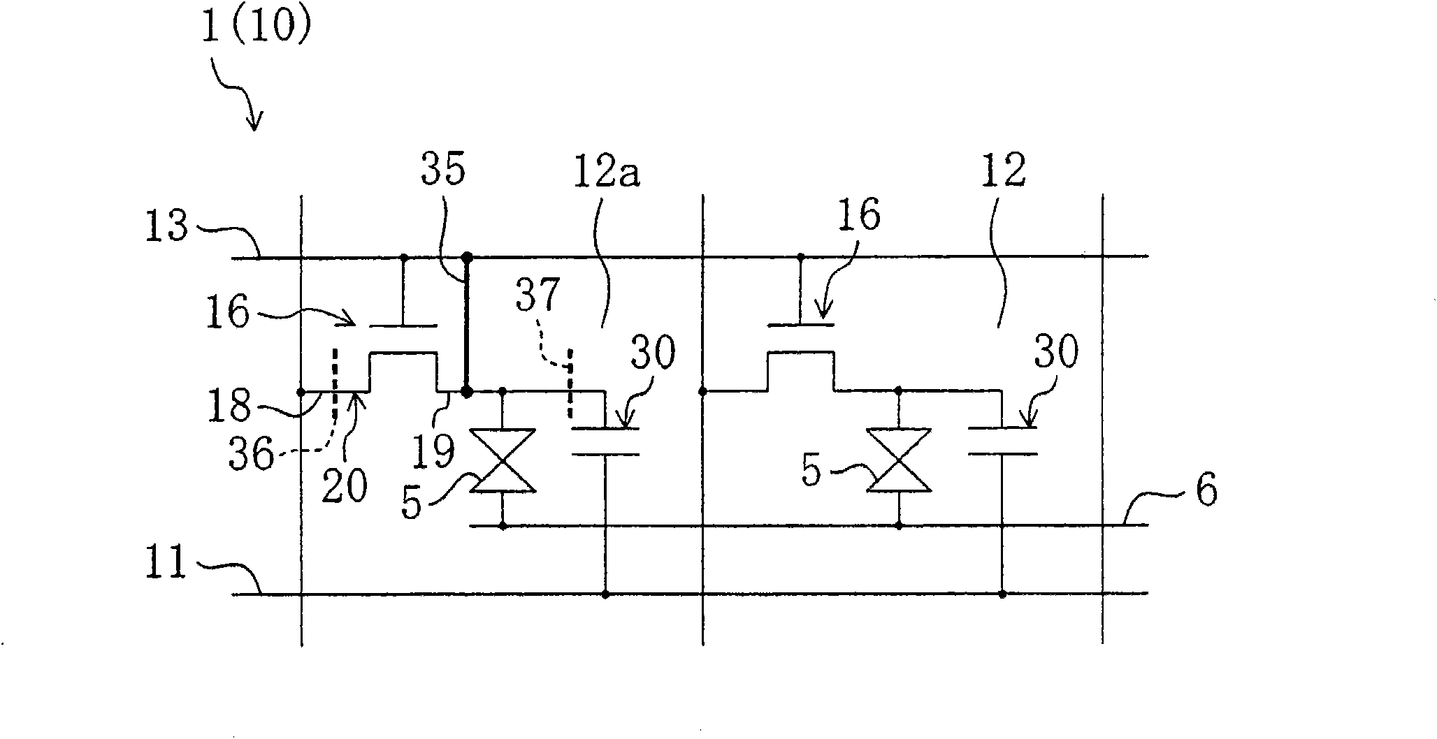
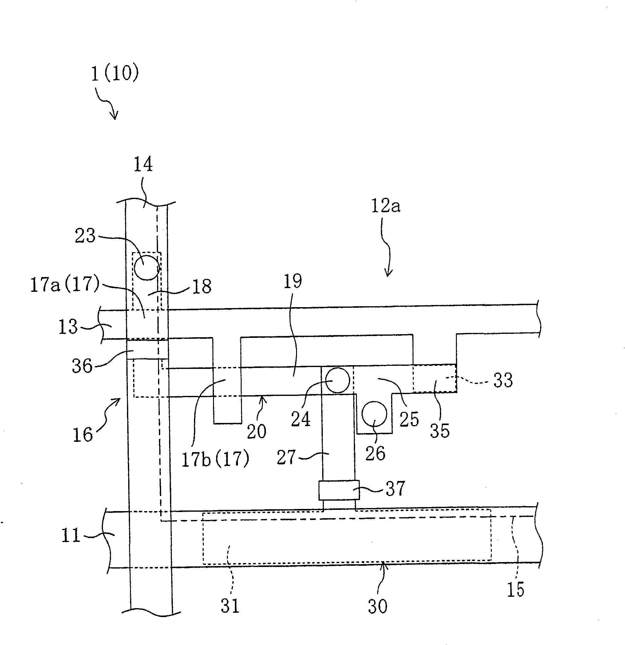
[0081] figure 1 and figure 2 Embodiment 1 of this invention is shown. In Embodiment 1, a liquid crystal display device will be described as an example of a display device. figure 1 It is a circuit diagram showing the configuration of the liquid crystal display device 1 in the first embodiment. figure 2 It is an enlarged plan view showing a part of the correction pixel in the first embodiment.
[0082] The liquid crystal display device 1 is an active matrix type liquid crystal display device, and it includes: a TFT substrate 10, an opposite substrate (not shown) arranged opposite to the TFT substrate 10, and a substrate disposed between the above-mentioned opposite substrate and the above-mentioned TFT substrate 10. Liquid crystal layer 5. In addition, the liquid crystal display device 1 is a normally white liquid crystal display device that performs white display with no voltage applied to the liquid crystal layer 5 and black display with a voltage applied to the liquid ...
Embodiment approach 2
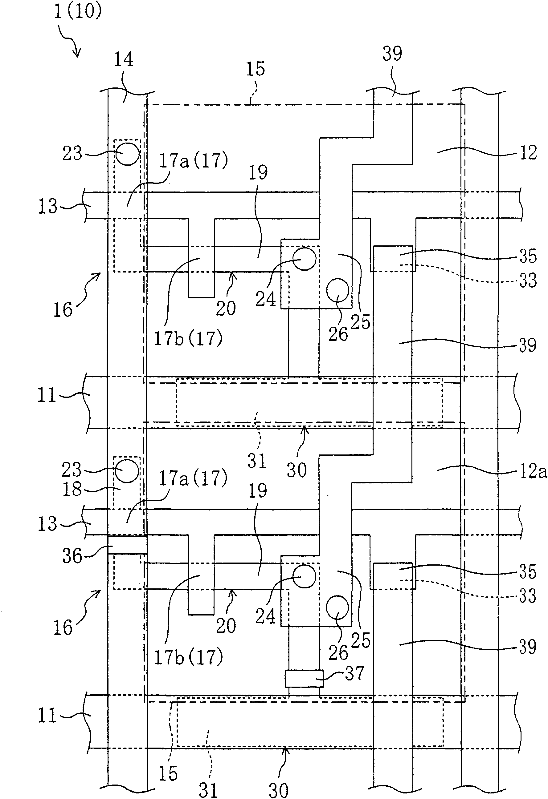
[0117] image 3 with Figure 4 Embodiment 2 of this invention is shown. image 3 It is an enlarged plan view showing two pixels in the second embodiment. Figure 4 is a plan view schematically showing a pixel arrangement. In addition, in each of the following embodiments, for the figure 1 with figure 2 The same parts are denoted by the same reference numerals, and detailed description thereof will be omitted.
[0118] In the first embodiment described above, the short-circuit portion 35 is formed in the correction pixel 12a, but in the second embodiment, the short-circuit portion 35 is formed in a pixel 12 different from the correction pixel 12a.
[0119] That is, the drain portion 19 of the correction pixel 12a is short-circuited with the gate line 13 connected to the TFT 16 of the pixel 12 adjacent to the correction pixel 12a. The pixel 12 in which the short-circuit portion 35 is formed is adjacent to the correction pixel 12 a via the CS wiring 11 . That is, the gate...
Embodiment approach 3
[0131] Figure 5 Embodiment 3 of this invention is shown. Figure 5 It is an enlarged plan view showing a part of correction pixels in Embodiment 3. FIG.
[0132] In the first embodiment described above, the short-circuit region 33 is formed on the gate wiring 13 , whereas in the third embodiment, the short-circuit region 33 is formed on the gate electrode 17 of the TFT 16 .
[0133]That is, if Figure 5 As shown, in the pixel 12 , the short-circuit region 33 is extended from the front end of the gate electrode 17 of the TFT 16 . The width of the short-circuit region 33 in the longitudinal direction of the gate wiring 13 is larger than that of the gate electrode 17 . On the other hand, part of the drain electrode 25 is extended so as to overlap the short-circuit region 33 and faces the short-circuit region 33 . Thus, in the correction pixel 12a, the short-circuit portion 35 is formed in the short-circuit region 33 described above.
[0134] According to such a configuratio...
PUM
 Abstract
Description
Claims
Application Information


