Method for chip alignment

A technology for wafers and alignment marks, which is applied in the fields of electrical components, semiconductor/solid-state device manufacturing, circuits, etc., and can solve the problems of complicated error values, error values ​​on the wafer carrier, and increased measurement errors, etc.

Active Publication Date: 2010-07-28
NAN YA TECH
View PDF0 Cites 11 Cited by
  • Summary
  • Abstract
  • Description
  • Claims
  • Application Information

AI Technical Summary

Problems solved by technology

[0005] Since the above-mentioned alignment marks and overlay marks are measured in two different machines (the exposure machine and the overlay machine), however, the wafer stages, detectors, etc. There is an error value, if two different machines are used, it will complicate the measurement error value and increase the overall measurement error

Method used


Image

  • Method for chip alignment
  • Method for chip alignment
  • Method for chip alignment

Examples


Embodiment Construction

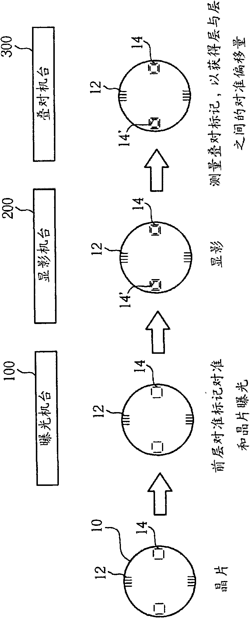
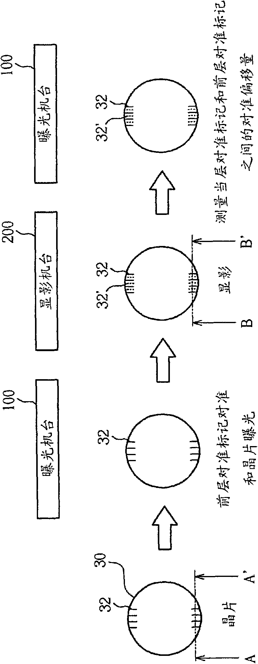
[0021] figure 1 is a schematic diagram of a known wafer alignment method.

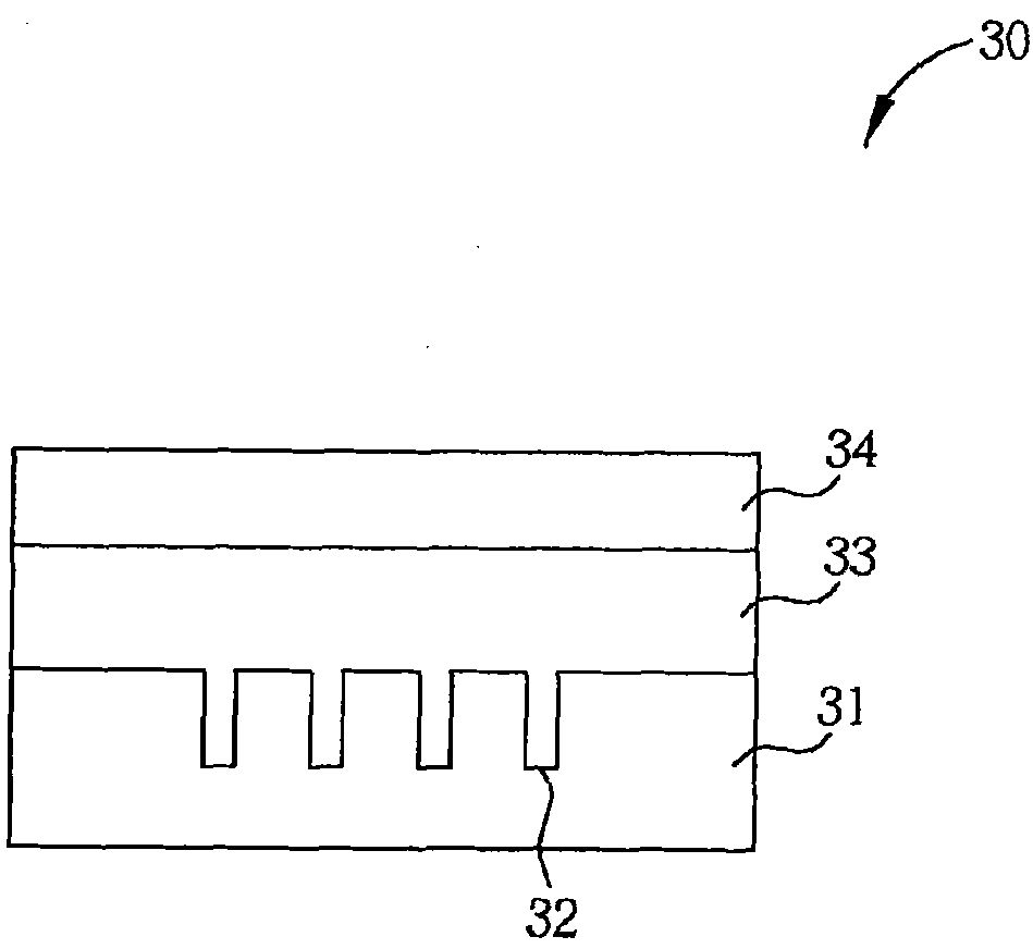
[0022] Such as figure 1 As shown, at first a wafer 10 is provided, on which a first material layer (not shown), a second material layer (not shown) and a third material layer (not shown) are sequentially arranged from bottom to top, the first material layer layer and the second material layer may be a silicon substrate, a conductive layer or an insulating layer, and the third material layer may be photoresist. In the first material layer on the wafer 10, alignment marks 12 and overlay marks 14 are provided. The alignment mark 12 and the overlay mark 14 may be groove structures recessed in the first material layer, and are disposed at the edge of the wafer or on the dicing line. Next, the wafer 10 is sent into the exposure machine 100, and the alignment marks 12 are used to align the wafer 10 before exposure, so that the wafer 10 is placed in a suitable exposure position, and then the wafer 10 is irr...


PUM


Abstract

The invention provides a method for chip alignment, which comprises: firstly, providing a chip comprising a first material layer and a second material layer, wherein the second material layer is positioned on the first material layer and the first material layer has a first alignment mark; secondly, in a lithography machine, measuring the position of the first alignment mark; thirdly, patterning the second material layer and forming a second alignment mark by using the patterned second material layer; and finally, in the aerator, measuring the offset between the second alignment mark and the first alignment mark. In the invention, the relative position error between the material layers is measured by using the alignment marks, and the measurement result is not influenced by the error between different machines as the whole measurement is performed in the same lithography machine rather than the traditional overlay tool.

Description

technical field [0001] The invention relates to a wafer alignment method in semiconductor technology, in particular to a method for increasing alignment precision. Background technique [0002] In the semiconductor process, there are many processing steps, such as exposure, development, and etching. In these steps, in order to form the desired integrated circuit components, the circuit patterns between the various material layers on the wafer must have accurate relative positions. Therefore, in various processing procedures, appropriate marks are provided to increase alignment accuracy. [0003] Before the wafers are formally mass-produced, a small number of wafers are usually used for testing first, using the alignment marks set on the wafers. Before exposure, the placement position of the wafers in the exposure machine is determined using the front layer ( pre-layer) alignment marks for alignment. The front layer refers to the material layer that has been processed in t...

Claims


Application Information

Patent Timeline
Patent Type & Authority Applications(China)
IPC IPC(8): H01L21/68
Inventor 刘安雄
Owner NAN YA TECH
Why Eureka
Try Eureka