Device and method for determining optimal focal plane position of lithography machine

A technology of the best focal plane and lithography machine, which is applied in the photolithography process exposure device, the microlithography exposure equipment, the photolithography process of the pattern surface, etc. question

Inactive Publication Date: 2010-08-11
INST OF OPTICS & ELECTRONICS - CHINESE ACAD OF SCI
View PDF4 Cites 17 Cited by
  • Summary
  • Abstract
  • Description
  • Claims
  • Application Information

AI Technical Summary

Problems solved by technology

Not only greatly reduces the production efficiency, but also has a great impact on the imaging quality of the lithography device

Method used


Image

  • Device and method for determining optimal focal plane position of lithography machine
  • Device and method for determining optimal focal plane position of lithography machine
  • Device and method for determining optimal focal plane position of lithography machine

Examples


Embodiment Construction

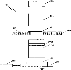
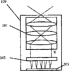
[0041] like figure 1As shown, the device for measuring the best focal plane position of a lithography machine according to the embodiment of the present invention includes a light source 101, an illumination system 102, mask tables 103, 105, a mask 104, a silicon wafer 106, a workpiece table 107, an optical imaging system 108, wave aberration sensor 109, and interferometer 110. The light source 101 is a deep ultraviolet laser light source that generates light beams. The illumination system 102 shapes the light beams to produce desired light beams. The workpiece table 107 carries and positions the silicon wafer 106. The optical imaging system 108 has a projection objective lens 1081. The optical system images the mask image on the silicon wafer. On the sheet 106 , a wave aberration sensor 109 is located on the workpiece table 107 to measure the wave aberration of the projection objective lens 1081 , and the interferometer 110 is used to position the work table 107 . The light ...


PUM


Abstract

The invention provides a measuring device for determining the optimal focal plane position of a lithography machine and a method thereof. The device comprises an illuminated light source system, a projection objective imaging system, a masking table, a workbench, a wave aberration sensor and an interferometer for precisely positioning, wherein the masking table is sued for supporting and fixing a mask plate, and the workbench is used for supporting and fixing a wafer. The method deduces the conversion relationship between outoffocus and other image differences, a wave aberration sensor detects the wave aberration of an optical imaging system on different out-of-focus positions, and the optimal focal plane position of the lithography machine can be obtained by calculation according to a measuring result. The measuring device and the method of the invention can measure the optimal focal plane position of the lithography machine.

Description

technical field [0001] The invention relates to a photolithography device, in particular to a device and method for determining the best focal plane position of the photolithography device. Background technique [0002] Lithography equipment is mainly used in the manufacture of integrated circuits IC or other micro-devices. A mask pattern can be imaged on a photoresist-coated wafer, such as a semiconductor wafer or an LCD panel, by means of a photolithographic apparatus. The lithography device is exposed through the projection objective lens, and the involved mask pattern is transferred to the photoresist. The projection objective lens is the core component of a lithography device, and its imaging quality is a key factor affecting the resolution of lithography. [0003] In order to obtain the best imaging effect, at the time of exposure, the upper surface of the wafer coated with photoresist should be placed at the height of the best focal plane. Therefore, in the system ...

Claims


Application Information

Patent Timeline
Patent Type & Authority Applications(China)
IPC IPC(8): G03F9/00G03F7/20
Inventor 陈红丽邢廷文廖志杰林妩媚
Owner INST OF OPTICS & ELECTRONICS - CHINESE ACAD OF SCI
Why Eureka
Try Eureka