Substrate for holding at least one component and method for producing same
What is Al technical title?
Al technical title is built by PatSnap Al team. It summarizes the technical point description of the patent document.
A technology for substrates and components, applied in semiconductor/solid-state device manufacturing, electrical components, electrical solid-state devices, etc., can solve problems such as DCB substrate fracture, and achieve the effect of simple cost
Inactive Publication Date: 2010-08-18
SEMIKRON ELECTRONICS GMBH & CO KG
View PDF0 Cites 2 Cited by
Summary
Abstract
Description
Claims
Application Information
AI Technical Summary
This helps you quickly interpret patents by identifying the three key elements:
Problems solved by technology
Method used
Benefits of technology
Problems solved by technology
This bending may lead to breakage of the DCB substrate in other processing chains
Method used
Image
Click on the blue label to locate the original text in one second.
Reading with bidirectional positioning of images and text.
Examples
Embodiment Construction
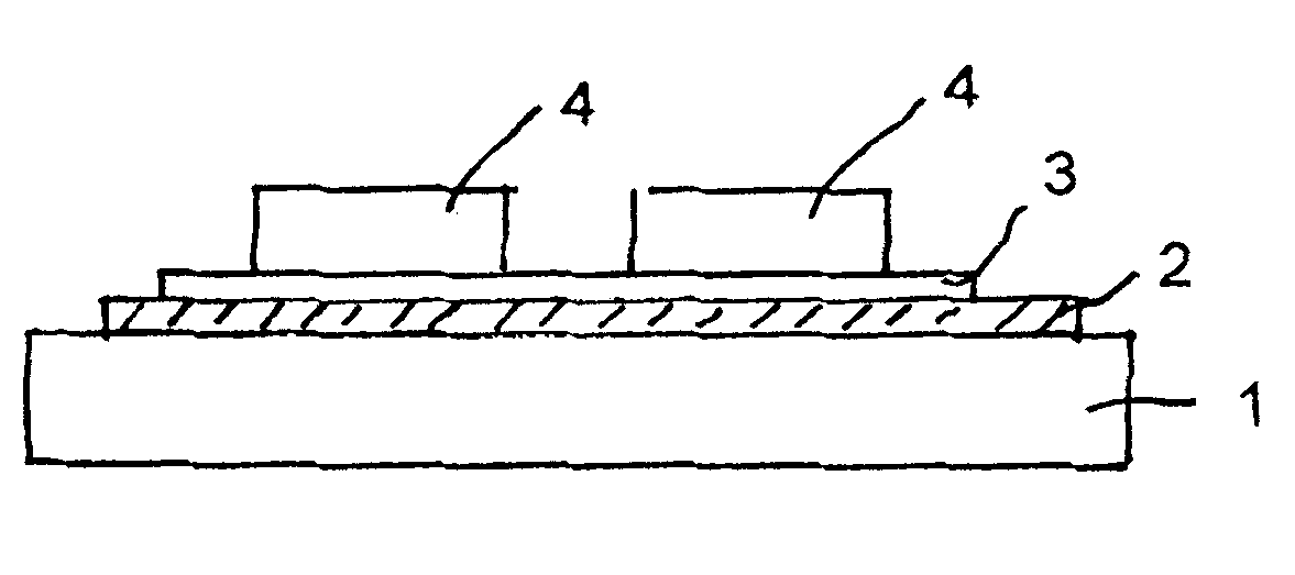
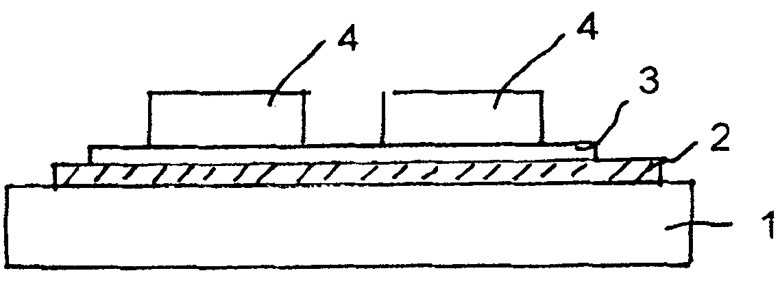
[0027] exist figure 1 In this case, a connection layer 2 is provided on the substrate body 1 . The connection layer 2 connects the conductive layer 3 with the substrate body 1 . The conductive layer 3 is connected to the element 4, and the conductive layer 3 may be a conductor line structure. The component 4 can be a semiconductor component, in particular a power semiconductor. The element 4 is connected to the conductive layer 3 , for example by means of a conventional solder connection.
[0028] The connection layer 2 is electrically insulating, preferably made of polysiloxane, which is filled with fillers up to a filling degree of 60% by volume to 80% by volume. The filler is suitably SiC having an average particle size in the range of 2 to 10 μm. Such a connection layer 2 has an excellent thermal conductivity λ of greater than 20 W / mK.
[0029] The substrate body 1 is made of metal, preferably a copper alloy or an aluminum alloy. The substrate body 1 can be produced ...
PUM
Abstract
The invention relates to a substrate for holding at least one component and method for producing the same, the component (4) is specially a power semiconductor, the substrate has a substrate body (1) provided at the front and rear sides with an electrically conductive layer (3, 3a, 3b). For improving the thermal conductivity of the electrically conductive layer (3, 3a, 3b), an electrically insulated connection layer (2, 2a, 2b) is provided between the substrate body (1) and the electrically conductive layer (3, 3a, 3b), which has a duroplastic matrix formed from the pre-ceramic polymer. In the method for producing the substrate, the electrically conductive layer (3, 3a, 3b), in the presence of the pre-ceramic polymer, is connected with the substrate body (1), then the pre-ceramic polymer is transformed into the thermosetting form, thereby the electrically insulated connection layer (2, 2a, 2b) is formed for connecting the electrically conductive layer (3, 3a, 3b) and the substrate body (1).
Description
technical field [0001] The invention relates to a substrate according to the preamble of claim 1 . The invention also relates to a method of manufacturing a substrate. Background technique [0002] Substrates for receiving electrical or electronic components are generally known from the prior art. Such a substrate generally consists of a plate of electrically insulating material which is provided with an electrically conductive layer at least on the front side and / or on the opposite rear side. The plate can be made of electrically insulating plastic or ceramic, for example. In particular for the production of modules equipped with power semiconductors, direct copper-on-copper (DCB) substrates are used according to the prior art, for example. Here, plates made of aluminum oxide or aluminum nitride are used as electrical insulators. As a result, the conductor lines are applied from pure copper in a high-temperature melting and diffusion process. Such DCB substrates are di...
Claims
Application Information
Patent Timeline
Application Date:The date an application was filed.
Publication Date:The date a patent or application was officially published.
First Publication Date:The earliest publication date of a patent with the same application number.
Issue Date:Publication date of the patent grant document.
PCT Entry Date:The Entry date of PCT National Phase.
Estimated Expiry Date:The statutory expiry date of a patent right according to the Patent Law, and it is the longest term of protection that the patent right can achieve without the termination of the patent right due to other reasons(Term extension factor has been taken into account ).
Invalid Date:Actual expiry date is based on effective date or publication date of legal transaction data of invalid patent.