Integrated package structure for super power vertical chip

An integrated packaging, ultra-high power technology, applied in the direction of electrical components, circuits, semiconductor devices, etc., can solve the problems of limiting packaging power density, uneven distribution of gold wires, etc., achieve high thermal conductivity, and realize the effect of stable power supply with large currents

Pending Publication Date: 2016-01-20
FUDAN UNIV +1
View PDF1 Cites 3 Cited by
  • Summary
  • Abstract
  • Description
  • Claims
  • Application Information

AI Technical Summary

Problems solved by technology

However, this structure also uses gold wires as the electrical connection carrier between the chip electrodes and the substrate. When the chip cur

Method used


Image

  • Integrated package structure for super power vertical chip
  • Integrated package structure for super power vertical chip
  • Integrated package structure for super power vertical chip

Examples


Embodiment Construction

[0018] The present invention will be further described below in conjunction with the accompanying drawings and embodiments. The described embodiments are only some of the embodiments of the invention. All other embodiments without creative achievements based on the embodiments of the present invention belong to the protection scope of the present invention.

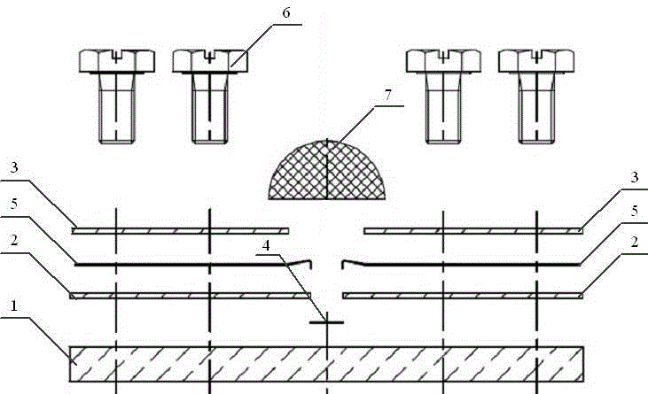
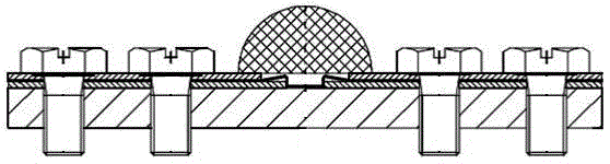
[0019] The integrated packaging structure of the ultra-high power vertical chip of the present invention, its assembly diagram is as follows figure 1 shown. The substrate of this packaging structure is composed of positive electrode conductive plate 1, insulating layer 2 and negative electrode conductive plate 3. The insulating layer 2 and the negative electrode conductive plate are slotted, and three UV LED vertical chips 4 rated at 35W are arranged in a straight line in the groove. The P-type electrode below the chip is eutectically welded to the positive conductive plate 1 , and the N-type electrode above the chip is...


PUM


Abstract

The invention belongs to the technical field of semiconductor lighting devices, and in particular discloses an integrated package structure for a super power vertical chip. In the integrated package structure, a metal foil is used for connecting a negative electrode pad of the super power vertical chip and a base electrode, and a high current steady load and a high heat conducting property of the chip are achieved. A package base comprises a positive electrode conductive plate, a negative electrode conductive plate and an insulating heat conducting layer. Eutectic soldering is adopted between the negative electrode pad of the vertical chip and the metal foil, between the metal foil and the negative electrode conductive plate, and between the positive electrode of the chip and the positive electrode conductive plate. By replacing a gold wire or an aluminum wire connecting the negative electrode of the chip and the negative electrode of the package base with the metal foil, the invention solves the problem of difficulty in high current conduction between the LED chip and the package base, improves the heat dissipating performance of the package, achieves reliable high power density package, and can be used for super power LED ultraviolet, visible and infrared lighting systems.

Description

technical field [0001] The invention belongs to the technical field of semiconductor lighting devices, and in particular relates to an integrated package structure of a super-high-power vertical chip. Background technique [0002] With the rapid development of LED chip preparation technology, the power of a single chip is increasing, which promotes the development of various high-power or high-power-density LED devices and lighting systems, and expands the application of LED in various general lighting and special lighting. The field and scope of application. Especially in the field of ultraviolet LED applications, the input power of a single chip with a wavelength above 365nm has increased from a few watts to tens of watts, and is developing towards a hundred watts. [0003] Vertical structure chips are an inevitable trend in the development of high-power chips. The P-type and N-type electrodes of the vertical structure LED chip are on both sides of the LED epitaxial laye...

Claims


Application Information

Patent Timeline
IPC IPC(8): H01L33/62H01L33/64H01L33/48
CPCH01L33/48H01L33/62H01L33/647
Inventor 张善端韩秋漪荆忠
Owner FUDAN UNIV
Why Eureka
Try Eureka