Stacked multi-encapsulation structure device, semiconductor encapsulation structure and manufacturing method thereof

A manufacturing method, semiconductor technology, applied in the direction of semiconductor/solid-state device manufacturing, semiconductor devices, semiconductor/solid-state device components, etc., can solve the problem of not being able to reduce the risk of solder overflow, not having openings, and not being able to reduce the possibility of short circuits between lines, etc. problem, achieve the effect of reducing the risk of solder overflow, reducing the possibility, and avoiding the deviation of package structure

Inactive Publication Date: 2010-08-18
ADVANCED SEMICON ENG INC
View PDF1 Cites 5 Cited by
  • Summary
  • Abstract
  • Description
  • Claims
  • Application Information

AI Technical Summary

Problems solved by technology

[0006] However, the lower encapsulation compound 117 of the lower package structure 110 of the known stacked multi-package structure device 150 does not have any openings, which surrounds and exposes the pads 115 or the solder balls 128
Therefore, the known stacked multi-package structure device 150 cannot reduce the risk of solder extrusion after soldering (solder extrusion risk), and thus cannot reduce the possibility of short circuits between lines.

Method used


Image

  • Stacked multi-encapsulation structure device, semiconductor encapsulation structure and manufacturing method thereof
  • Stacked multi-encapsulation structure device, semiconductor encapsulation structure and manufacturing method thereof
  • Stacked multi-encapsulation structure device, semiconductor encapsulation structure and manufacturing method thereof

Examples


Embodiment Construction

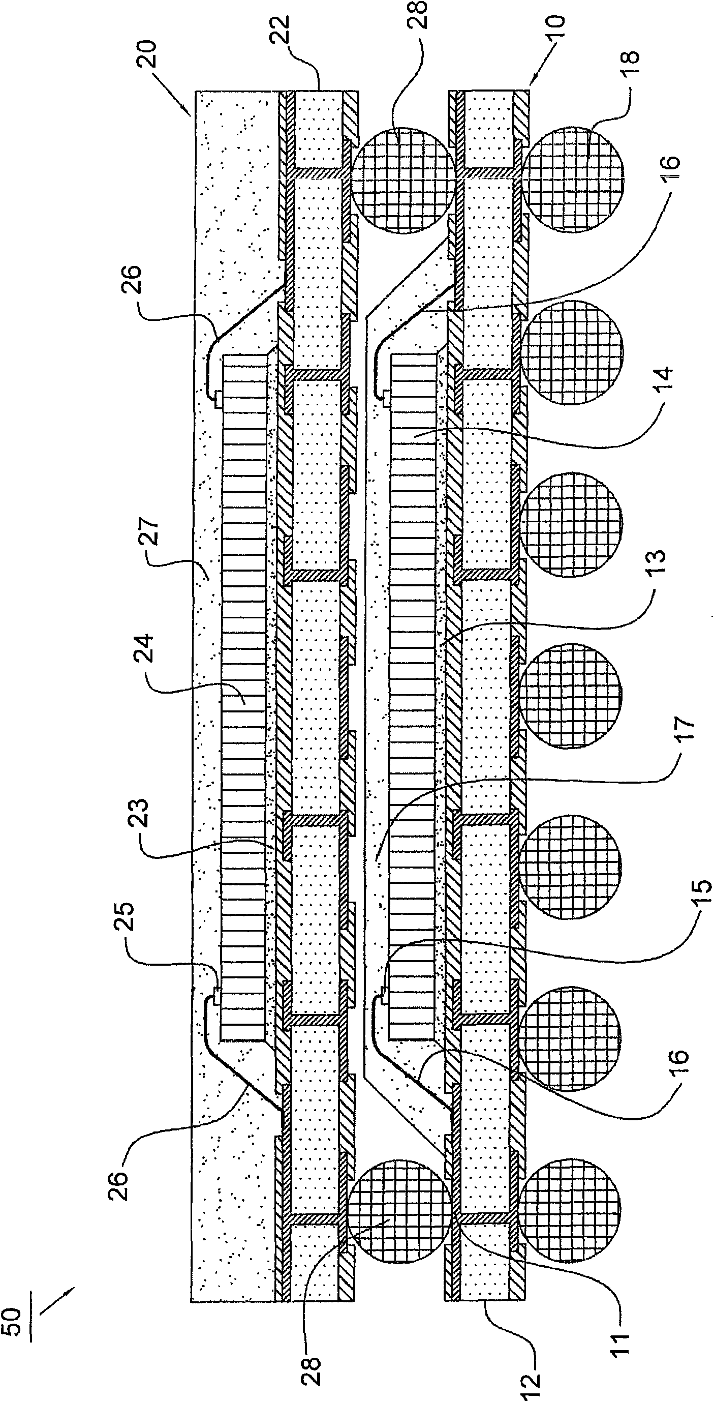
[0069] refer to image 3 , which shows a stacked multi-package construction device (Package On Package; POP) 200 according to the first embodiment of the present invention. The stacked multi-package structure device 200 includes a lower package structure 210 and an upper package structure 220 .

[0070] The lower packaging structure 210 includes a first chip 214 fixed and electrically connected to an upper surface 242 of a first substrate 212 . The first substrate 212 has an upper metal layer and a lower metal layer, which can be patterned to provide appropriate circuitry, and are electrically connected to each other through plated through holes. An interposer 230 can be fixed on the first chip 214 via glue 232 and electrically connected to the upper surface 242 of the first substrate 212 . The intermediary substrate 230 can be a circuit board or a substrate. The intermediary substrate 230 has an upper surface 236 and a lower surface 238 , the lower surface 238 is opposite t...


PUM


Abstract

The invention relates to a semiconductor encapsulation structure which comprises a baseplate, a chip and a sealant compound; wherein the baseplate contains a plurality of electric contacts which are positioned on the upper surface of the baseplate; the chip is fixedly and electrically connected to the upper surface of the baseplate; and the sealant compound covers the baseplate and the chip and exposes out of the lower surface of the baseplate, wherein the sealant compound contains a plurality of openings, and each opening encloses and exposes out of each electric contact.

Description

technical field [0001] The present invention relates to a stacked multi-package structure device, and more particularly to a lower package structure of a stacked multi-package structure device. The sealing compound has an opening to surround and expose the electrical contacts of the substrate. Background technique [0002] At present, the stacked multi-package structure (Package on Package; POP) device mainly refers to disposing one semiconductor package structure on another semiconductor package structure, and its basic purpose is to increase the density to produce greater functions per unit space and better regional performance, thereby reducing the total area and cost of the entire stacked multi-package construction device. [0003] Referring to FIG. 1, U.S. Patent No. 7,101,731, entitled "Semiconductor multi-package module having inverted second package stacked over die-up flip-chip ball grid array (BGA) package), its prior art discloses the structure of a stacked multi...

Claims


Application Information

Patent Timeline
Patent Type & Authority Applications(China)
IPC IPC(8): H01L23/31H01L21/56
CPCH01L2924/15311H01L2924/1815H01L2224/73265H01L2924/15321H01L2224/48227H01L2224/32225H01L2924/19107H01L24/73H01L2924/00012H01L2924/00
Inventor 朱吉植翁承谊廖振凯
Owner ADVANCED SEMICON ENG INC
Why Eureka
Try Eureka