Optimal design method of multilayer diffraction optical element
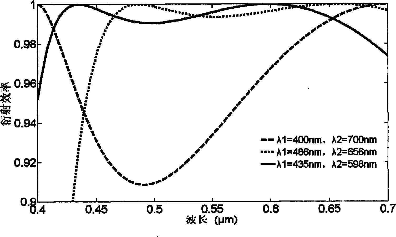
A diffractive optical element, optimized design technology, applied in diffraction grating and other directions, can solve the problem of not considering the bandwidth integral diffraction efficiency, etc., to maximize the bandwidth integral average diffraction efficiency, the surface microstructure height is small, and the optimization selection problem can be solved.
Inactive Publication Date: 2010-08-25
CHANGCHUN UNIV OF SCI & TECH
View PDF1 Cites 7 Cited by
- Summary
- Abstract
- Description
- Claims
- Application Information
AI Technical Summary
Problems solved by technology
The design wavelength of the multilayer diffractive optical element in the visible light band is selected as F light and C light, or the two ends of the wave band, and the height of the surface microstructure of the multilayer diffractive optical element is calculated through the design wavelength and the selected optical material. Does not consider whether the bandwidth-integrated average diffraction efficiency is the maximum
Method used
View moreImage
Smart ImageViewing Examples
Examples
Embodiment Construction
Login to View More PUM
 Abstract
The invention relates to an optimal design method of a multilayer diffraction optical element, which belongs to the technical field of optical design. The optimal design is not realized in the prior art. The method comprises the following steps of: (1) optimally selecting an optical material of the multilayer diffraction optical element according to a surface microstructure height formula of the multilayer diffraction optical element; (2) determining the bandwidth integration average diffraction efficiency distribution by using different design wavelength combinations in the entire working waveband; (3) determining the greatest bandwidth integration average diffraction efficiency and the relative design wavelength in the entire working waveband; and (4) substituting the design wavelength corresponding to the greatest bandwidth integration average diffraction efficiency into the surface microstructure height formula of the multilayer diffraction optical element, and calculating out the optimal surface microstructure height and the optimal design wavelength of the multilayer diffraction optical element. The method is used for designing the multilayer diffraction optical element used for a wide-waveband imaging optical system, and maximizes the bandwidth integration average diffraction efficiency of the multilayer diffraction optical element.
Description
Optimal Design Method for Multilayer Diffractive Optical Elements technical field The invention relates to an optimal design method of a multilayer diffractive optical element, which is used for the design of a multilayer diffractive optical element in a wide-band imaging optical system. The method can realize the maximum and quantitative The optimized design can improve the imaging quality of a refraction / diffraction hybrid optical system containing multilayer diffractive optical elements, and belongs to the technical field of optical design. Background technique With the development of optical manufacturing technology, diffractive optical elements have created an independent branch in modern optics, bringing revolutionary changes to traditional optical design theory and manufacturing processes. Diffractive optical elements can be used to correct various imaging defects such as chromatic aberration and aberration, bringing more design freedom and wide material options to ...
Claims
Login to View More Application Information
Patent Timeline
 Patent Type & Authority Applications(China)
IPC IPC(8): G02B5/18
Inventor 薛常喜崔庆丰
Owner CHANGCHUN UNIV OF SCI & TECH


