Liquid crystal display device and manufacturing method thereof

A liquid crystal display and device technology, applied in the field of liquid crystal displays, can solve problems that affect the brightness and contrast of the display screen, reduce the clarity of the display screen, and reduce the light transmittance of the liquid crystal panel.

Inactive Publication Date: 2011-11-30
BOE TECH GRP CO LTD +1
View PDF0 Cites 0 Cited by
  • Summary
  • Abstract
  • Description
  • Claims
  • Application Information

AI Technical Summary

Problems solved by technology

However, in the specific use process, the inventor found that attaching a film with touch function on the liquid crystal panel will reduce the light transmittance of the liquid crystal panel, which will affect the technical indicators such as brightness and contrast of the display screen, and will also reduce the display screen. clarity of

Method used


Image

  • Liquid crystal display device and manufacturing method thereof
  • Liquid crystal display device and manufacturing method thereof
  • Liquid crystal display device and manufacturing method thereof

Examples


Embodiment 1

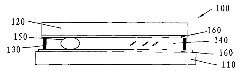
[0038] An embodiment of the present invention provides a liquid crystal display device, such as Figure 4 and Figure 5 As shown, the thin film transistor array substrate of the liquid crystal display device includes gate scan lines 420 and data scan lines 410 intersecting each other on the substrate 456, The thin film transistor 450 is switched, and a pixel electrode 440 is also included in the area defined by the intersection of the gate scan line 420 and the data scan line 410 . The cross-sectional structure of the switching thin film transistor 450 is as follows Figure 5 As shown, the switching thin film transistor 450 includes a gate 451 connected to the gate scanning line 420, a source 452 connected to the data scanning line 410, a drain 453 connected to the pixel electrode 440, and a gate electrode 453 overlapping with the gate scanning line 420 and The semiconductor layer 459 a defines the channel 454 between the source electrode 452 and the drain electrode 453 . A...

Embodiment 2

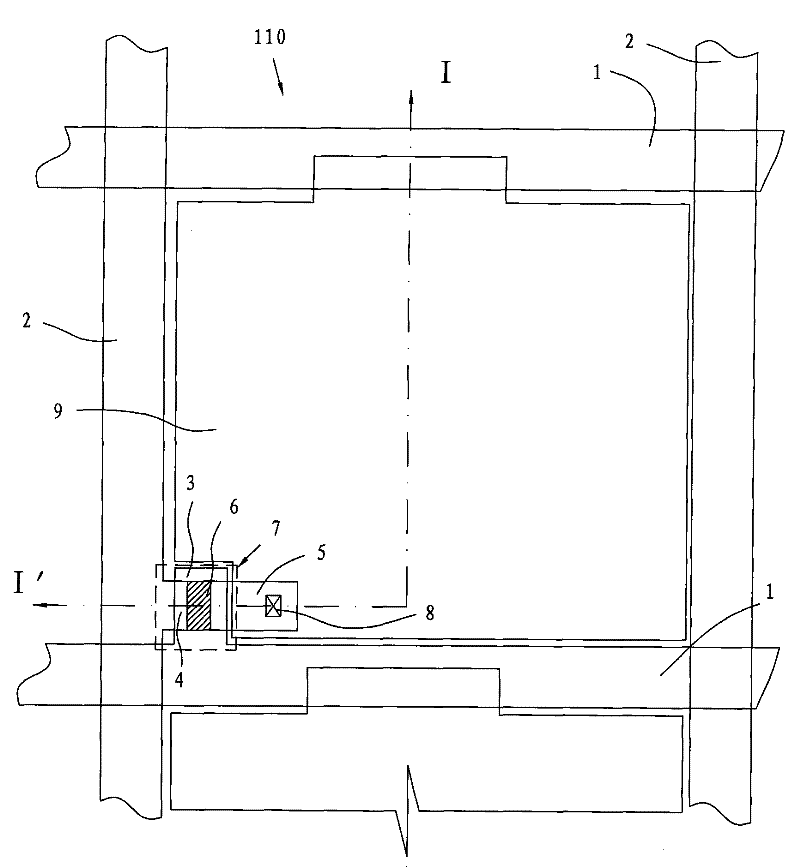
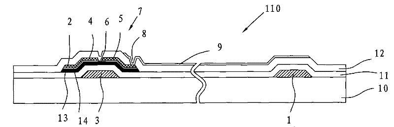
[0050] An embodiment of the present invention provides a method for manufacturing a liquid crystal display device. In the process of manufacturing a TFT array substrate, a photosensitive thin film transistor and a signal line parallel to a data scanning line are formed while manufacturing a switching thin film transistor; The source and gate of the light-sensitive thin film transistor are connected to one of the gate scanning lines that define the pixel unit, and the drain is output to the signal line; then an auxiliary barrier with a reflective layer on the surface is prepared on the color filter glass substrate A spacer, the auxiliary spacer is correspondingly disposed directly above the channel of the light-sensing thin film transistor, and there is a space reserved between the light-sensing thin film transistor and the light-sensing thin film transistor.

[0051] In order to convert the photocurrent generated by the photosensitive thin film transistor into a more obvious si...


PUM


Abstract

The invention discloses a liquid crystal display device and a manufacturing method thereof, relates to the field of liquid crystal displays, and solves the problem that the existing liquid crystal display device with a touch function affects the brightness, contrast and clarity of a display screen. In the embodiment of the present invention, a signal line and a light-sensitive thin film transistor are added to the liquid crystal display device, and an auxiliary spacer with a gap therebetween is arranged on the light-sensitive thin film transistor. The surface of the auxiliary spacer has a light-reflecting layer; wherein the light-sensitive thin film The drain of the transistor needs to be output to the signal line, and the gate and source of the light-sensing thin film transistor are both connected to the gate scanning line. The embodiments of the present invention are mainly used in liquid crystal displays, especially liquid crystal displays with touch function.

Description

technical field [0001] The invention relates to the field of liquid crystal displays, in particular to a liquid crystal display device in a liquid crystal display with touch function, and a manufacturing method of the liquid crystal display device. Background technique [0002] A liquid crystal display includes pixel units arranged in a matrix, and a driving circuit for driving the pixel units, and uses an electric field to control light transmittance of liquid crystals to display images. Such as figure 1 As shown, the liquid crystal display device 100 includes a thin film transistor (TFT, Thin Film Transistor) array substrate 110 and a color filter glass substrate 120 facing each other, and the two substrates are sealed to the box by a sealant 130 to form the liquid crystal display device 100, and Both the TFT array substrate 110 and the color filter glass substrate 120 are coated with an alignment layer 160; the liquid crystal display device 100 also includes a liquid cry...

Claims


Application Information

Patent Timeline
Patent Type & Authority Patents(China)
IPC IPC(8): G02F1/1362H01L27/12H01L21/84
Inventor 王峥黄应龙
Owner BOE TECH GRP CO LTD
Why Eureka
Try Eureka