InAs/GaSb superlattice infrared photoelectric detector for HPT (Hydrogenated Propylene Tetramer) structure

An electrical detector and superlattice technology, applied in circuits, electrical components, semiconductor devices, etc., can solve problems such as application limitations and high cost

Active Publication Date: 2012-01-04
INST OF SEMICONDUCTORS - CHINESE ACAD OF SCI
View PDF0 Cites 0 Cited by
  • Summary
  • Abstract
  • Description
  • Claims
  • Application Information

AI Technical Summary

Problems solved by technology

[0003] However, the most commonly used silicon-doped detectors, InSb, QWIP, MCT and other infrared detectors are required to work at low temperatures, require special refrigeration equipment, and are expensive, so their applications are limited.

Method used


Image

  • InAs/GaSb superlattice infrared photoelectric detector for HPT (Hydrogenated Propylene Tetramer) structure
  • InAs/GaSb superlattice infrared photoelectric detector for HPT (Hydrogenated Propylene Tetramer) structure

Examples


Embodiment Construction

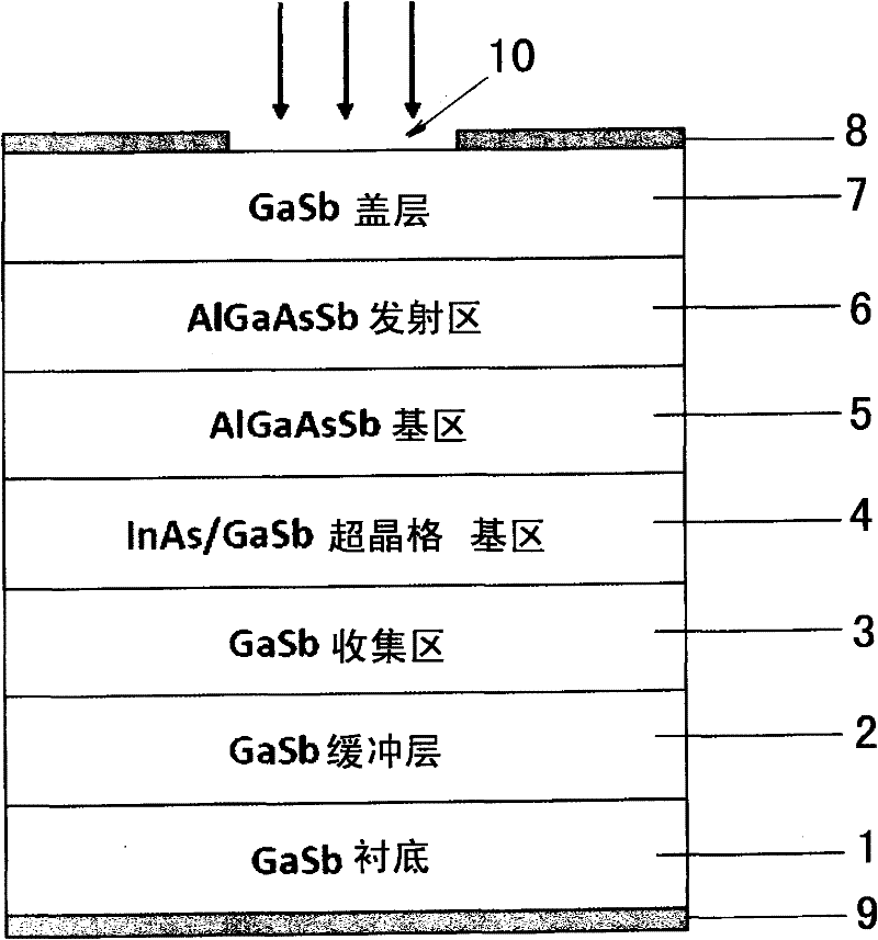
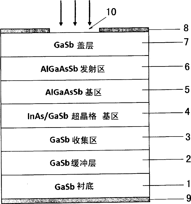
[0019] see figure 1 As shown, the invention provides a kind of InAs / GaSb superlattice infrared photodetector of HPT structure, comprising:

[0020] A GaSb substrate 1, a GaSb buffer layer 2, a GaSb collection region 3, an InAs / GaSb superlattice base region 4, a base region 5 formed of AlGaAsSb, and an AlGaAsSb emitter region are sequentially prepared on the GaSb substrate 1 by molecular beam epitaxy 6 and GaSb capping layer 7;

[0021] Wherein the GaSb collection region 3 is n-doped with a thickness of 1.5um;

[0022] The InAs / GaSb superlattice base region 4 described therein is composed of no less than 300 InAs layers / GaSb layers with a period of 1 micron grown alternately; wherein the thickness of each layer of GaSb is 3nm, and the thickness of each layer of InAs is determined by the detection wavelength . The InAs / GaSb superlattice base region 4 is used as the light absorption region of the HPT structure, and its function is to convert the incident optical signal into an...


PUM


Abstract

The invention relates to an InAs / GaSb superlattice infrared photoelectric detector for an HPT (Hydrogenated Propylene Tetramer) structure, which comprises a GaSb substrate, a top electrode and a bottom electrode, wherein a GaSb buffer layer, a GaSb collecting region, a InAs / GaSb superlattice base region, a AlGaAaSb base region, a AlGaAaSb emitting region and a GaSb covering layer are respectivelyprepared on the GaSb substrate by using a molecular beam epitaxy method; the top electrode is prepared on the surface of the GaSb covering layer by using a sputtering method, and a light entrance port is arranged in the center of the top electrode; and the bottom electrode is prepared on the lower surface of the GaSb substrate by using a sputtering method.

Description

technical field [0001] The invention relates to semiconductor technology, mainly an InAs / GaSb superlattice infrared detector with HPT structure grown on a GaSb substrate. Background technique [0002] With the advancement of science and technology, infrared detectors with military use as the core have gradually developed. Atmospheric monitoring and other military and civilian fields have a wide range of applications. [0003] However, the most commonly used silicon-doped detectors, InSb, QWIP, MCT and other infrared detectors are required to work at low temperatures, require special refrigeration equipment, and are expensive, so their applications are limited. The InAs / GaSb infrared detector is due to the particularity of its materials, for example: the high effective mass of electrons and holes can effectively reduce the tunneling current and increase the density of states; the energy difference between the heavy hole band and the light hole band is large It can reduce Au...

Claims


Application Information

Patent Timeline
Patent Type & Authority Patents(China)
IPC IPC(8): H01L31/11
Inventor 张宇王国伟汤宝任正伟徐应强牛智川陈良惠
Owner INST OF SEMICONDUCTORS - CHINESE ACAD OF SCI
Why Eureka
Try Eureka