
Method for manufacturing lateral double-diffused metal oxide semiconductor transistor

An oxide semiconductor and lateral double-diffusion technology, applied in semiconductor/solid-state device manufacturing, semiconductor devices, electric solid-state devices, etc., can solve the problems of complex process and high cost, simplify process integration, simplify manufacturing process, and improve device channel effect of track length

Active Publication Date: 2012-11-14
SILERGY SEMICON TECH (HANGZHOU) CO LTD
View PDF0 Cites 0 Cited by
  • Summary
  • Abstract
  • Description
  • Claims
  • Application Information

AI Technical Summary

Problems solved by technology

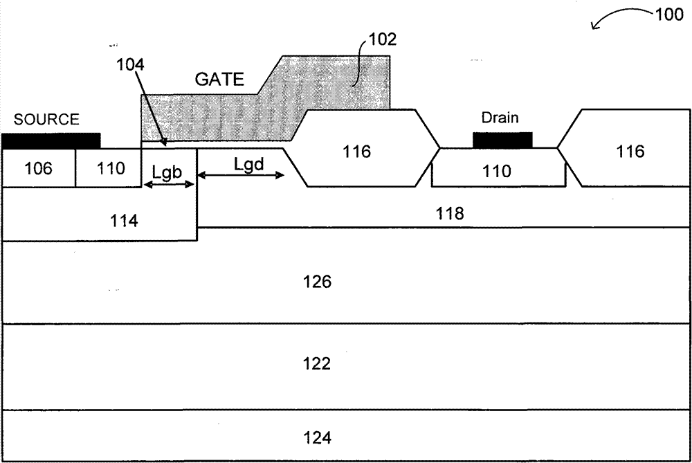
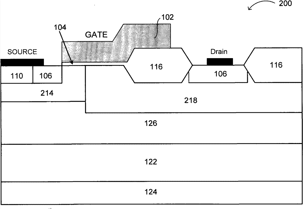
[0005] In view of the above-mentioned defects, the object of the present invention is to provide a lateral double-diffused metal-oxide-semiconductor transistor, as well as its manufacturing method and application, so as to solve the problems of complicated process and high cost in the prior art.

Method used


Image

  • Method for manufacturing lateral double-diffused metal oxide semiconductor transistor
  • Method for manufacturing lateral double-diffused metal oxide semiconductor transistor
  • Method for manufacturing lateral double-diffused metal oxide semiconductor transistor

Examples


Embodiment Construction

[0047] Several preferred embodiments of the present invention will be described in detail below with reference to the accompanying drawings, but the present invention is not limited to these embodiments. The present invention covers any alternatives, modifications, equivalent methods and schemes made on the spirit and scope of the present invention. In order to provide the public with a thorough understanding of the present invention, specific details are set forth in the following preferred embodiments of the present invention, but those skilled in the art can fully understand the present invention without the description of these details. In addition, well-known methods, procedures, procedures, components, circuits, etc. have not been described in detail in order to avoid unnecessary confusion to the essence of the present invention.

[0048] The content of the present invention will be described below in the form of processes, processes, logic modules, functional modules, p...


PUM


Abstract

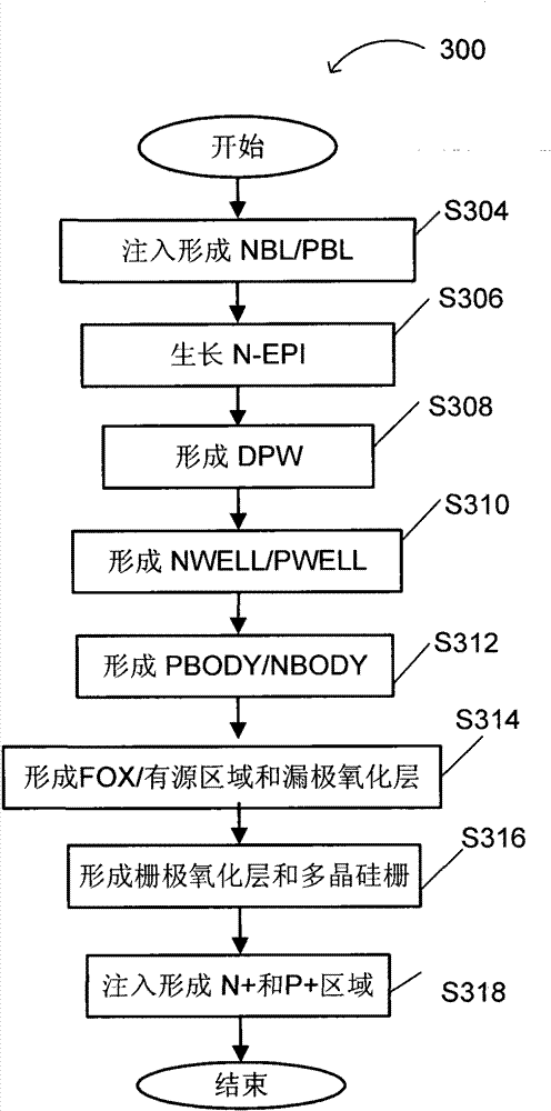
The invention relates to a lateral double-diffused metal oxide semiconductor transistor, namely an LDMOS transistor, and a structure, a manufacturing method and application. According to one embodiment of the invention, the method for manufacturing the LDMOS transistor with a source electrode region, a drain electrode region and a grid region on a substrate, includes: generating a P-typed bury layer region and a n-typed bury layer region, growing an external layer on the NBL / PBL region, forming a p-doped deep p-well region on the PBL region, forming a well region on the external layer, forming a doped body region, then forming a active region and a field oxidation region and forming a drain oxidation layer between the LDMOS transistor source region and the drain region, after the form of the doped body region, forming a grid oxidation layer approaching the source and drain region and forming a grid on the grid oxidation layer and one part of drain oxidation layer, then forming a dopeddrain region, and a first doped source region and a second doped source region.

Description

technical field [0001] The present invention relates to the field of semiconductor devices. More specifically, embodiments in accordance with the present invention relate to lateral double diffused metal oxide semiconductor transistors (LDMOS). Background technique [0002] Voltage regulators, such as DC-DC converters, are used to provide a stable voltage source for a wide variety of electronic systems. High efficiency DC-DC converters are especially required for battery management of low voltage devices such as laptops, mobile phones, etc. Switching voltage regulators generate a DC output voltage by converting an input DC voltage to a high frequency voltage, which is then filtered. Specifically, a switching regulator consists of a switch that alternately connects and disconnects a DC input voltage source (such as a battery) and a load (such as an integrated circuit IC), an output filter, and a controller. . The output filter typically includes an inductor and a capacito...

Claims


Application Information

Patent Timeline
Patent Type & Authority Patents(China)
IPC IPC(8): H01L21/336H01L29/78H01L27/02
CPCH01L29/66659H01L29/0878H01L21/823814H01L29/1095H01L29/66681H01L29/7816H01L29/42368H01L27/0922H01L29/1083H01L21/823892H01L29/7835
Inventor 游步东
Owner SILERGY SEMICON TECH (HANGZHOU) CO LTD
Learn More