Chip structure, wafer structure and chip fabrication technique

A technology of chip structure and manufacturing process, applied in semiconductor/solid-state device manufacturing, electrical components, electrical solid-state devices, etc., can solve problems such as chip fragmentation, and achieve the effect of improving cutting yield

Active Publication Date: 2010-10-06
ADVANCED SEMICON ENG INC
View PDF0 Cites 6 Cited by
  • Summary
  • Abstract
  • Description
  • Claims
  • Application Information

AI Technical Summary

Problems solved by technology

However, the wafer still needs to be removed from the carrier after dicing, and chip fragments are prone to occur during and after the removal process

Method used


Image

  • Chip structure, wafer structure and chip fabrication technique
  • Chip structure, wafer structure and chip fabrication technique
  • Chip structure, wafer structure and chip fabrication technique

Examples


Embodiment Construction

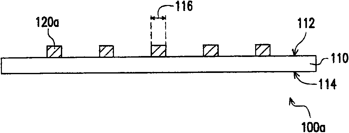
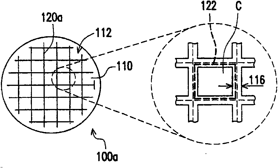
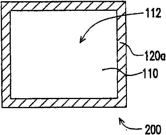
[0021] Figure 1A is a schematic cross-sectional view of a wafer structure according to an embodiment of the present invention, Figure 1B for Figure 1A The top view schematic diagram and partial enlarged schematic diagram of the wafer structure, Figure 1C for cutting Figure 1A A schematic top view of a chip structure formed by the wafer structure. Please also refer to Figure 1A and Figure 1B , in this embodiment, the wafer structure 100a includes a substrate 110 and a stress buffer layer 120a.

[0022] Specifically, the substrate 110 has a first surface 112, a second surface 114 opposite to the first surface 112, and a plurality of dicing lines 116 separating the substrate 110 into a plurality of chip regions C, wherein the dicing lines 116 are formed by a A passivation layer (not shown) is defined by a region not covering the first surface 112 of the substrate 110 , and this region does not include a pad region (not shown) exposed by the passivation layer.

[0023] T...


PUM


Abstract

The invention relates to a chip structure, a wafer structure and a chip fabrication technique, wherein the chip structure comprises a substrate and a stress-buffering layer. The substrate is provided with a first surface and a second surface opposite from the first surface. The stress-buffering layer is arranged around the substrate, and is at least positioned on one of the first and the second surfaces of the substrate.

Description

technical field [0001] The present invention relates to a semiconductor structure and a semiconductor manufacturing process, in particular to a chip structure, a wafer structure and a chip manufacturing process. Background technique [0002] Before cutting the wafers produced by the semiconductor integrated circuit manufacturing process, the wafers are usually subjected to a thinning process to reduce the thickness of the wafers. After the wafer goes through the thinning process, the area-to-thickness ratio of the wafer becomes larger, so wafer fragments are prone to occur during the subsequent process of picking and placing the wafer, transporting the wafer by the machine, and cutting the wafer. Therefore, the thinned wafer needs to be adhered to a carrier to be supported by the carrier, which is beneficial to the subsequent manufacturing process. However, the wafer still needs to be removed from the carrier after dicing, and chip fragments are prone to occur during and af...

Claims


Application Information

Patent Timeline
Patent Type & Authority Applications(China)
IPC IPC(8): H01L23/29H01L23/482H01L21/768H01L21/321H01L21/78
Inventor 彭胜扬
Owner ADVANCED SEMICON ENG INC
Why Eureka
Try Eureka