Packaging technique and packaging structure

A packaging process and packaging structure technology, applied in the direction of semiconductor/solid-state device components, semiconductor devices, electrical components, etc., can solve problems such as fragmentation and reduce production yield, and achieve the effect of preventing fragmentation, reducing difficulty, and increasing strength

Inactive Publication Date: 2011-01-26
ADVANCED SEMICON ENG INC
View PDF0 Cites 8 Cited by
  • Summary
  • Abstract
  • Description
  • Claims
  • Application Information

AI Technical Summary

Problems solved by technology

Since the process capability of bonding chips to wafers using flip-chip bonding technology still has its limit value, when the thickness of the wafer used is less than the limit value of its process capability, chipping is prone to occur during the flip-chip bonding process situation, which reduces the production yield

Method used


Image

  • Packaging technique and packaging structure
  • Packaging technique and packaging structure
  • Packaging technique and packaging structure

Examples


Embodiment Construction

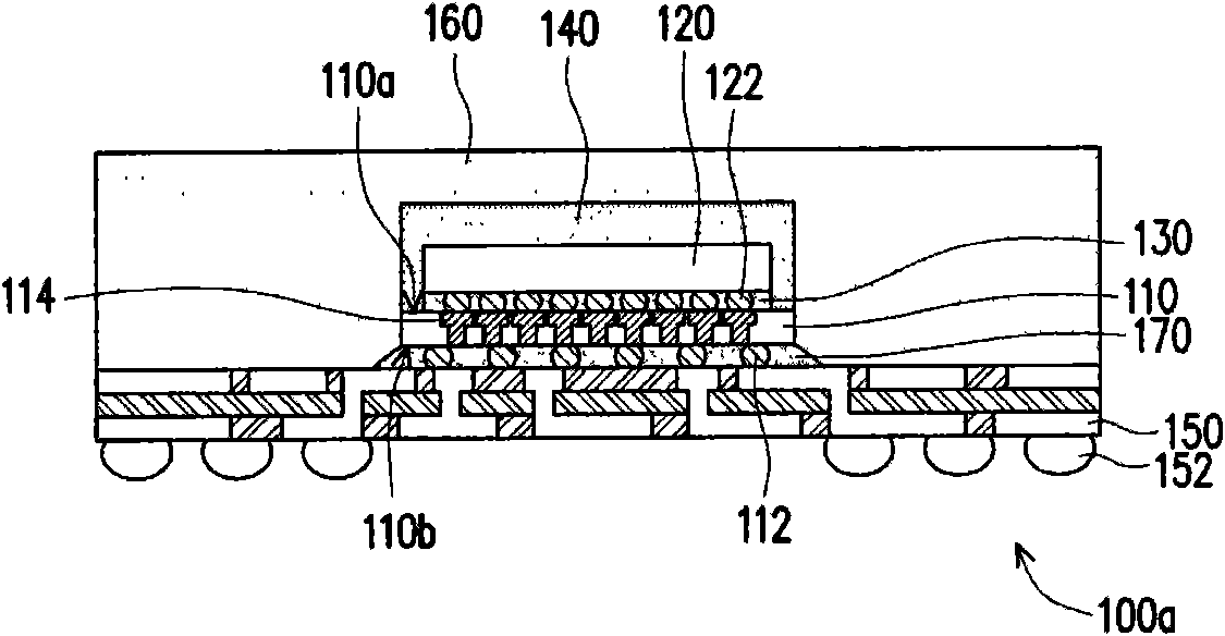
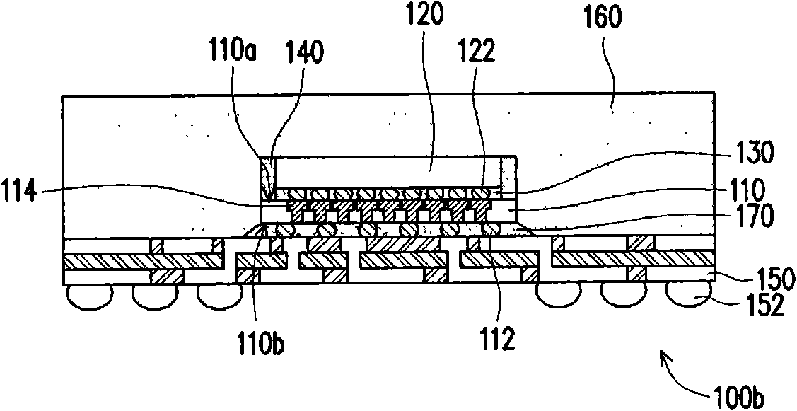
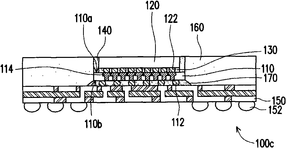
[0053] Figure 1A It is a schematic cross-sectional view of a package structure according to an embodiment of the present invention. Please refer to Figure 1A The packaging structure 100 a includes a semiconductor substrate 110 , a chip 120 , a first primer 130 and a first packaging compound 140 .

[0054]The semiconductor substrate 110 is, for example, a silicon substrate, which has an upper surface 110a, wherein the thickness of the semiconductor substrate 110 is less than 8 mils, such as less than 4 mils, or even 2 mils. The chip 120 is disposed on the upper surface 110 a of the semiconductor substrate 110 , and the bottom of the chip 120 has a plurality of first conductive bumps 122 . The first primer 130 is disposed between the semiconductor substrate 110 and the chip 120 to cover the first conductive bumps 122 . The first encapsulant 140 is disposed on the semiconductor substrate 110, and covers the side surfaces of the chip 120, the first primer 130, and the top surfa...


PUM


Abstract

The invention discloses a packaging technique and a packaging structure. According to the packaging technique, firstly a semiconductor substrate is configured on a carrier, the surface of which is provided with an adhesive layer, and is engaged with the carrier through the adhesive layer; then a chip is combined with the semiconductor substrate in an inverted way, and a first primer is formed between the chip and the semiconductor substrate to coat a plurality of first conductive bumps on the bottom of the chip; after that, a first packaging colloid is formed on the semiconductor substrate and at least coats the lateral surface of the chip and the first primer; finally, the semiconductor substrate, together with the chip on the semiconductor substrate and the first packaging colloid, is separated from the adhesive layer on the carrier to form an array packaging structure. According to the invention, the semiconductor substrate can be thin, and the packaging thickness can be reduced.

Description

technical field [0001] The invention relates to a semiconductor process and its structure, and in particular to a packaging process and a packaging structure. Background technique [0002] With the advancement of semiconductor and packaging technology, the production of micro-components such as micro-electromechanical components or optoelectronic components has also entered the stage of wafer-level packaging from the early chip-level packaging, in order to achieve the purpose of reducing packaging costs and light, thin, short and small . Specifically, wafer-level packaging takes wafers as the object of packaging processing, and its main purpose is to simplify the packaging process of chips to save time and cost. After the integrated circuit on the wafer is manufactured, the entire chip can be directly packaged, and then the wafer saw (wafer saw) is performed to form a plurality of chip packages respectively, and the finished chip package Can be mounted on circuit boards. ...

Claims


Application Information

Patent Timeline
Patent Type & Authority Applications(China)
IPC IPC(8): H01L21/50H01L21/58H01L21/56H01L21/304H01L21/78H01L23/13H01L23/482H01L23/31
CPCH01L2224/83005H01L23/3135H01L21/568H01L24/94H01L24/97H01L2224/13025H01L2224/14181H01L2224/16145H01L2224/16225H01L2224/32145H01L2224/32225H01L2224/73204H01L2224/81005H01L2224/94H01L2224/97H01L2924/15311H01L2924/18161H01L2924/14H01L2224/81H01L2224/83H01L2924/00
Inventor 沈启智陈仁川潘彦良
Owner ADVANCED SEMICON ENG INC
Why Eureka
Try Eureka