
Surge-resisting and anti-static light-emitting diode and manufacturing method thereof

A technology of light-emitting diodes and manufacturing methods, which is applied in the direction of circuits, electrical components, and electric solid-state devices, and can solve problems such as complex procedures, high manufacturing costs of light-emitting diodes, and reduced performance of light-emitting diodes in eliminating static electricity, so as to achieve simple procedures and improve protection breakthroughs. Waves and static electricity, increase the efficiency of eliminating surges and static electricity

Inactive Publication Date: 2010-10-13
裕星企业有限公司
View PDF2 Cites 4 Cited by
  • Summary
  • Abstract
  • Description
  • Claims
  • Application Information

AI Technical Summary

Problems solved by technology

[0005] Moreover, the existing antistatic light-emitting diodes are mainly gallium nitride-based light-emitting diodes, and the substrate of the light-emitting diodes is made of sapphire and other materials. However, the lattice constants of the gallium nitride-based semiconductor layer and the sapphire substrate do not match, so Causes a decrease in the static elimination performance of gallium nitride-based light-emitting diodes
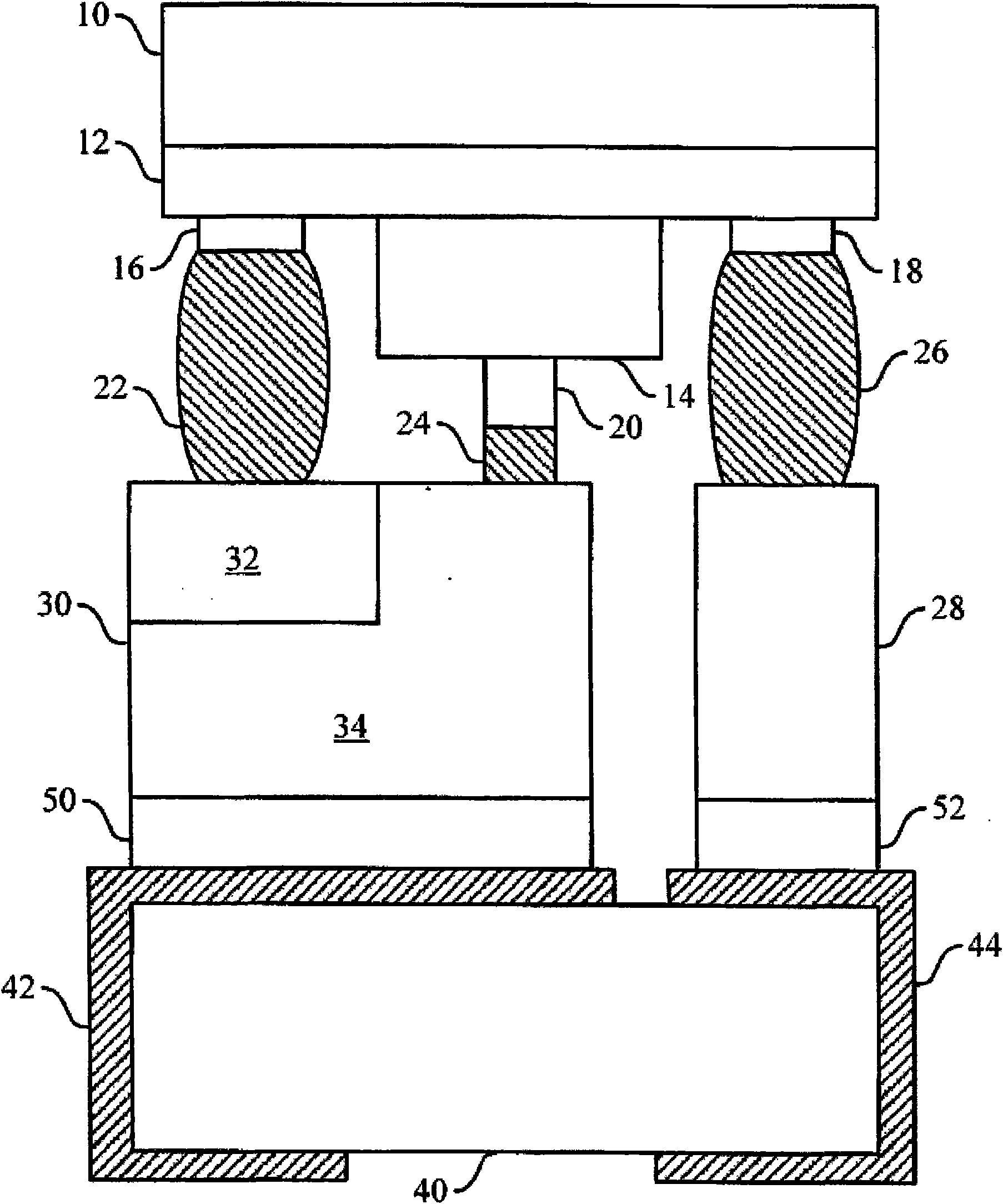
The most commonly used antistatic method today is to use a flip-chip packaging process, which forms a Zener diode combined with a light-emitting diode, which indeed solves the problem of light-emitting diodes in terms of static protection, but because of the process The procedure is quite complicated, and the more complicated the procedure in the manufacturing process, the higher the manufacturing cost of the LED

Method used


Image

  • Surge-resisting and anti-static light-emitting diode and manufacturing method thereof
  • Surge-resisting and anti-static light-emitting diode and manufacturing method thereof
  • Surge-resisting and anti-static light-emitting diode and manufacturing method thereof

Examples


Embodiment Construction

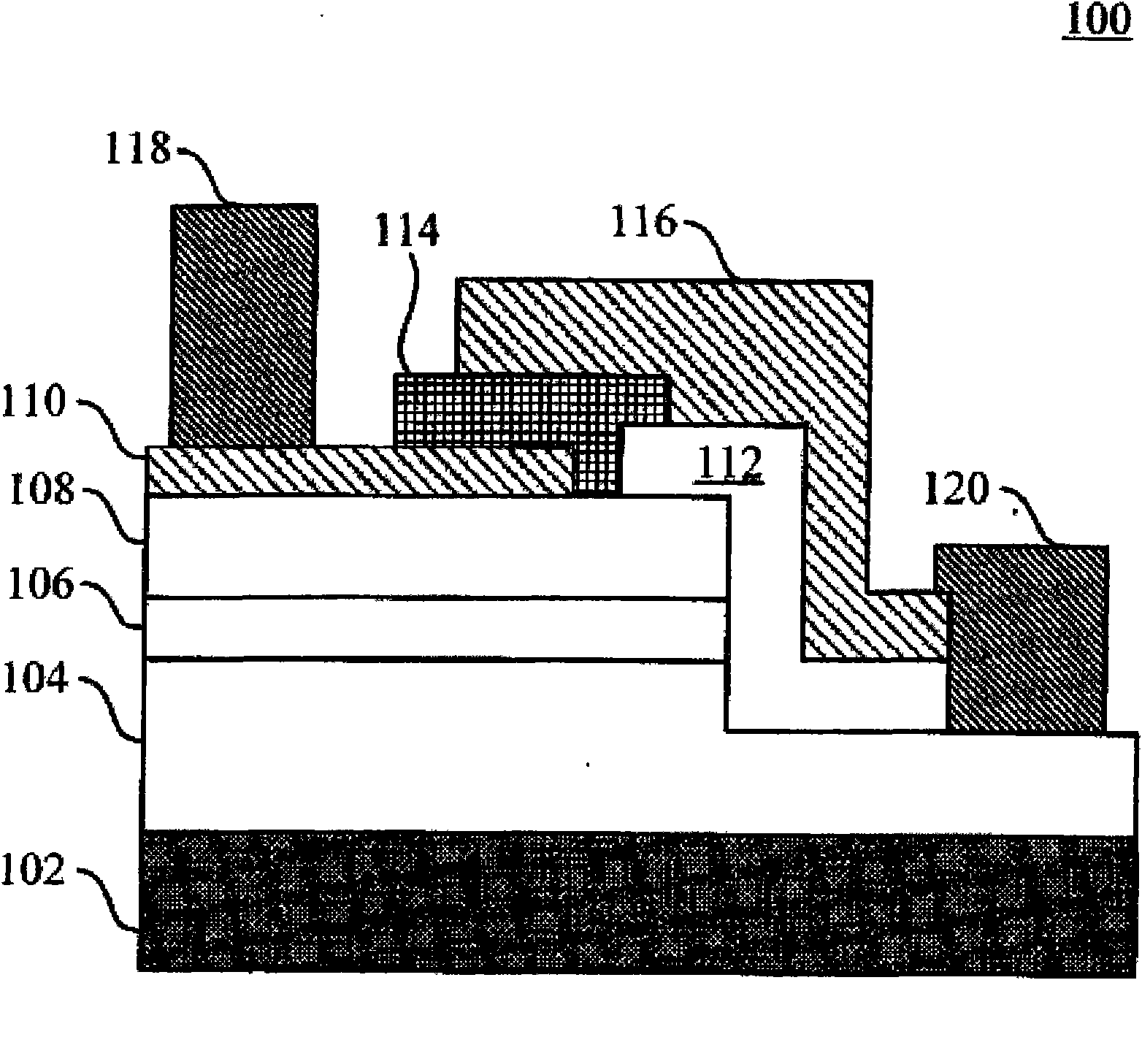
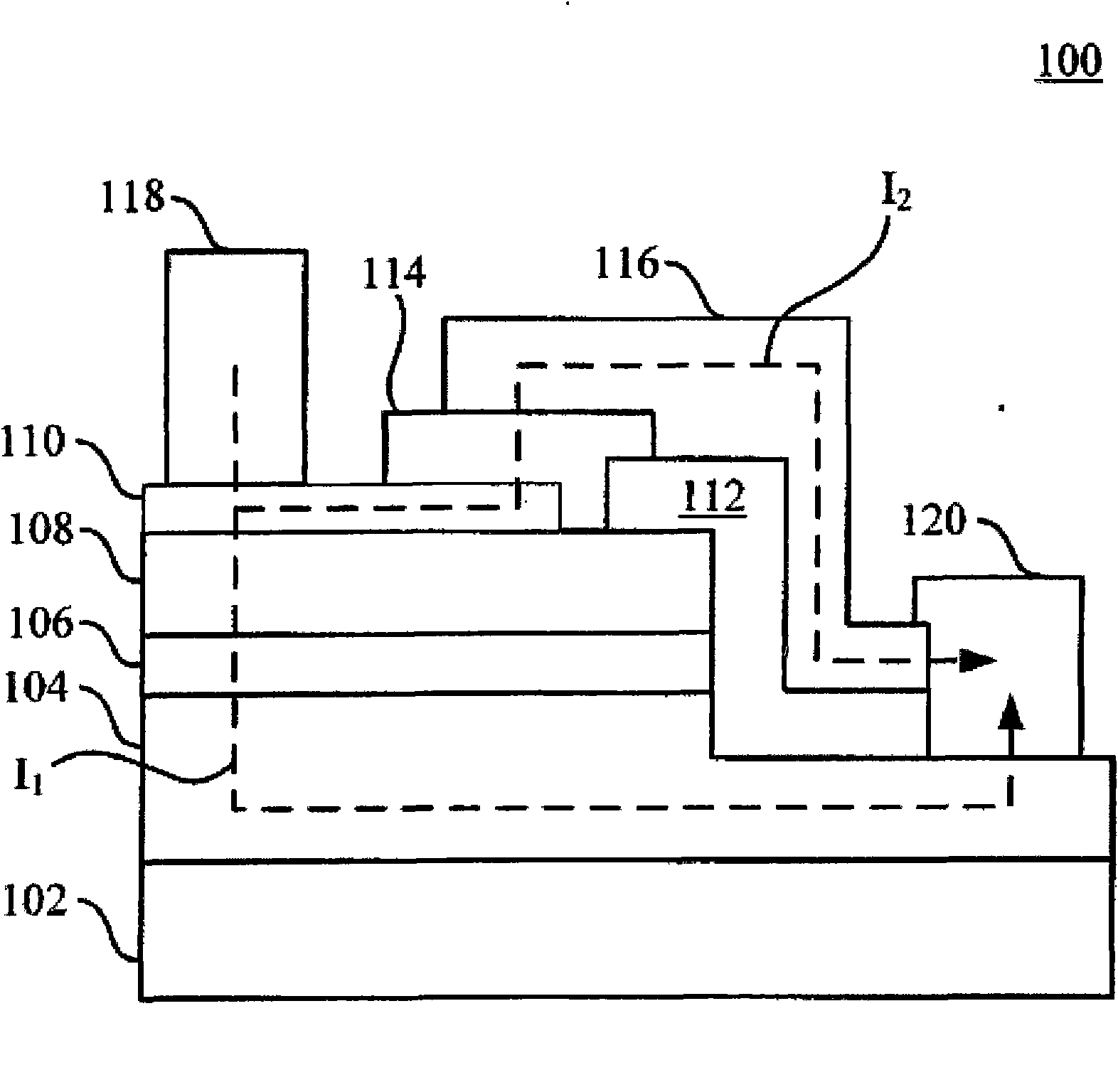
[0036] In the present invention, an oxide layer is formed on a diode chip, and when the diode receives a bias voltage exceeding the operating voltage, the oxide layer is used to promote the surge current derived from the bias voltage from the negative electrode through the second transparent conductive layer, oxidation Layer and the first transparent conductive layer conduct to the positive electrode and then lead out or conduct from the positive electrode to the negative electrode through the first transparent conductive layer, oxide layer and second transparent conductive layer and then lead out, so that the light-emitting diode can avoid the influence of surge and static electricity .

[0037] See figure 2 , is a side view of a light emitting diode according to a preferred embodiment of the present invention. As shown in the figure, the light emitting diode 100 of the present invention comprises a substrate 102, an N-type semiconductor layer 104, an active layer 106, a P-...


PUM


Abstract

The invention discloses a surge-resisting and anti-static light-emitting diode and a manufacturing method thereof. The light-emitting diode comprises a substrate, a N-type semiconductor layer, a P-type semiconductor layer, an active layer, a first transparent conductive layer, an oxide layer, an insulating layer, a second transparent conductive layer, a positive electrode and a negative electrode, wherein a first path for one voltage passing is formed from the positive electrode, the first transparent conductive layer, the P-type semiconductor layer, the active layer, the N-type semiconductor layer to the negative electrode, while a second path for one current passing is formed from the negative electrode, the oxide layer, the second transparent conductive layer to the positive electrode. When a bias voltage exceeds the operation voltage of the light-emitting diode, the surge current will flow from negative electrode to the positive electrode through the second path or from the positive electrode to the negative electrode through the second path so as to provide better surge-resisting and anti-static functions to the diode.

Description

technical field [0001] The invention relates to a photoelectric semiconductor structure and its manufacturing method, in particular to a light-emitting diode with anti-surge and static electricity and its manufacturing method. Background technique [0002] Today's optoelectronic semiconductor manufacturing process is mature, and has been further developed from the early micron process to the current nanometer process to improve the performance of optoelectronic semiconductor structures. One of the widely used optoelectronic semiconductor structures is light-emitting diodes, and the application of light-emitting diodes in Nowadays, it is more common in optoelectronic semiconductor manufacturing process, especially the application of light-emitting diodes and semiconductor lasers. However, as the manufacturing process of optoelectronic semiconductors is getting smaller and smaller, more attention should be paid to the overvoltage protection of diodes to prevent overcurrent cau...

Claims


Application Information

Patent Timeline
Patent Type & Authority Applications(China)
IPC IPC(8): H01L33/00H01L23/60
CPCH01L2224/16
Inventor 黄国钦潘锡明简奉任
Owner 裕星企业有限公司
Learn More