Organic electroluminescence device

An electroluminescent device and organic light-emitting layer technology, applied in organic semiconductor devices, circuits, electrical components, etc., can solve problems such as moisture ingress and cracks at the ends of pixel partition layers

Inactive Publication Date: 2010-10-13
SEIKO EPSON CORP
View PDF1 Cites 13 Cited by
  • Summary
  • Abstract
  • Description
  • Claims
  • Application Information

AI Technical Summary

Problems solved by technology

However, when trying to fabricate a film of this nature, due to the internal stress of the film itself, cracks will be generated at the end of the pixel partition wall layer, causing moisture to enter

Method used


Image

  • Organic electroluminescence device
  • Organic electroluminescence device
  • Organic electroluminescence device

Examples


no. 1 approach

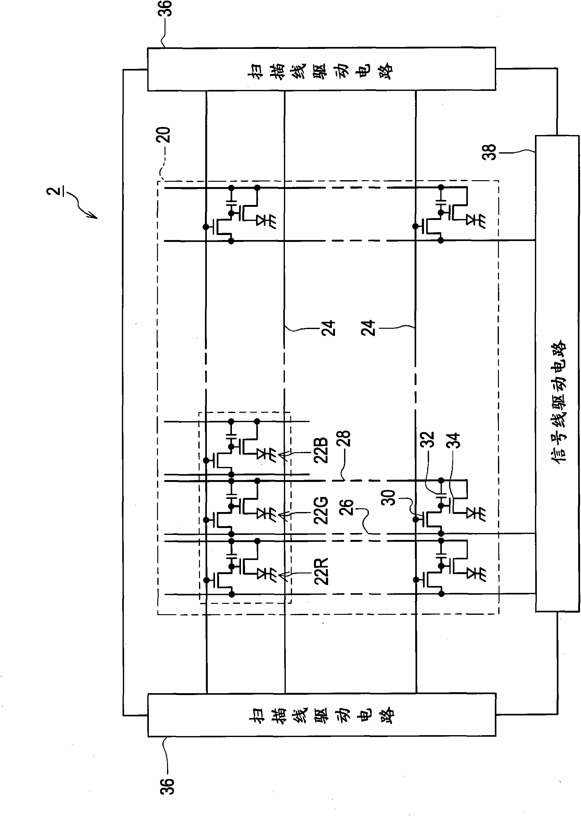
[0040] figure 1 It is an equivalent circuit diagram of various elements, wiring, and the like of the organic EL device 2 according to the present embodiment. In the display region 20 of the organic EL device 2, three types of organic EL elements, namely, a red organic EL element 22R emitting red light, a green organic EL element 22G emitting green light, and a blue organic EL element 22B emitting blue light, are regularly arranged. twenty two. Hereinafter, when the light emission color is not distinguished, it is simply referred to as the organic EL element 22 . In addition, as will be described later, the organic EL elements 22 differ only in the organic EL material that is the electro-optical material.

[0041] The organic EL device 2 is an active matrix type device that controls light emission of the organic EL elements 22 individually to form an image in the display area 20 including a plurality of organic EL elements 22 . A plurality of scanning lines 24 , a plurality ...

no. 2 approach

[0082] The structure of the organic buffer layer of the organic EL device according to this embodiment is the same as that of the common cathode layer in the first embodiment. However, the organic EL device according to this embodiment is a full-color panel using a low-molecular-weight organic EL material described later, and can perform full-color display using an organic EL element and a color filter that emit white light.

[0083] Figure 8 is a cross-sectional view of the organic EL device 4 according to this embodiment, Figure 9 will be Figure 8 Part B is an enlarged cross-sectional view shown. This organic EL device 4 includes a flat substrate 72 . The substrate 72 is made of glass or plastic, and a plurality of organic EL elements 74 are formed on the upper surface of the substrate 72 . The organic EL element 74 is an element that emits white light. The organic EL element 74 has an organic light-emitting layer 76 formed using a low-molecular-weight organic EL mate...

no. 3 approach

[0104] The organic EL device according to this embodiment is the same as the organic EL device 2 according to the first embodiment except for the structure of the organic buffer layer.

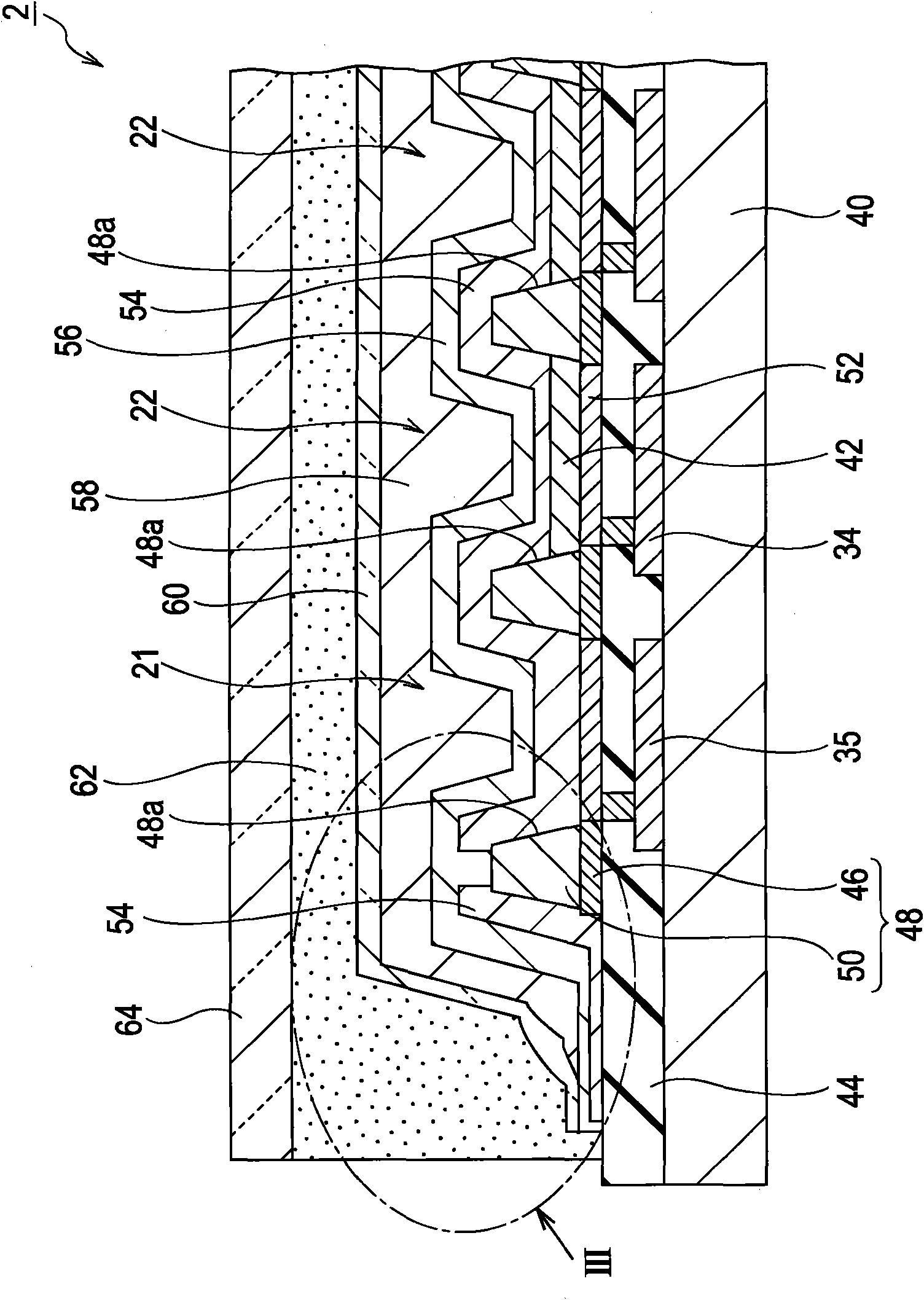
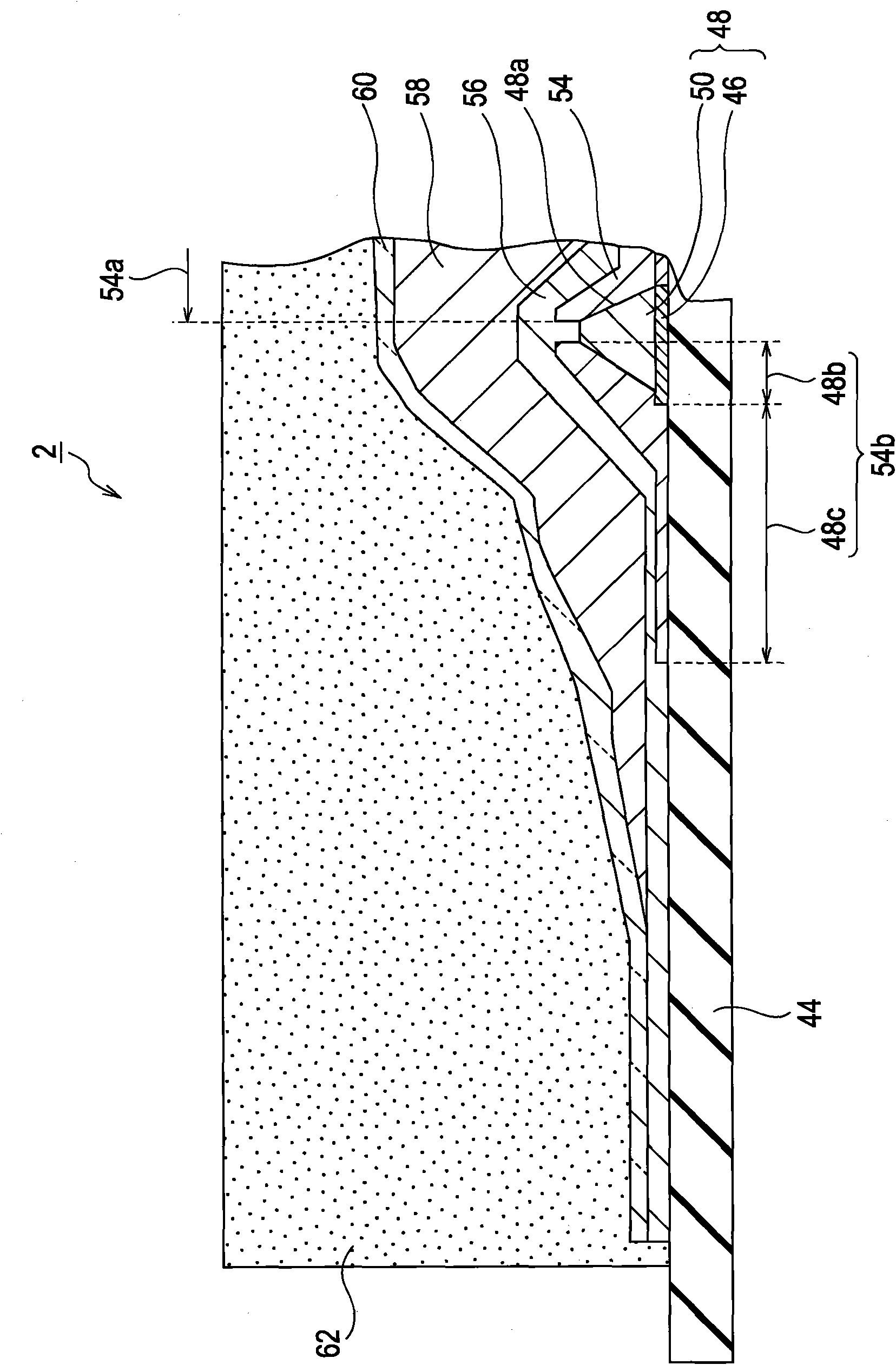
[0105] Figure 10 It is an enlarged cross-sectional view showing a part of the organic EL device 6 according to the present embodiment. In this organic EL device 6 , the first organic buffer layer 102 is formed on the cathodic protection layer 56 so as to overlap all of the plurality of organic EL elements 22 in order to flatten unevenness due to pixel partition walls. On the first organic buffer layer 102 , the second organic buffer layer 104 is formed so as to overlap all of the plurality of organic EL elements 22 . The gas barrier layer 60 is formed on the cathode protection layer 56 , the first organic buffer layer 102 , and the second organic buffer layer 104 so as to completely cover the terminals of the first organic buffer layer 102 and the second organic buffer layer 104 .

[0106] Th...


PUM


Abstract

The present invention provides an organic electroluminescence device which can improve humidity resistance performance and narrow a frame. The organic electroluminescence device includes on a substrate a plurality of first electrodes (52), a partition structure (48) having a plurality of openings (48a) corresponding to the positions of the first electrodes, an organic luminescent layer (42), a second electrode (54) covering the partition structure and the organic luminescent layer, and a sealing layer or a sealing member covering the second electrode. The second electrode includes a first portion (54a) and a second portion (54b) that are separate from each other. The first portion covers the entire partition structure (48b) except the outer portion from the edge of the partition structure, and the organic luminescent layer. The second portion covers the outer portion from the edge of the partition structure and at least part of the external region (48c) around the partition structure.

Description

technical field [0001] The present invention relates to an organic electroluminescent (Electro-Luminescence: hereinafter abbreviated as EL) device. Background technique [0002] A conventional organic EL device is constituted by forming an organic EL element on a substrate such as a glass substrate, and the organic EL element is composed of a laminate having an organic light-emitting layer (light-emitting layer formed of an organic material) between a pair of electrodes. . As the sealing method of this organic EL device, the following method can be mentioned: apply an epoxy-based adhesive on the laminate, and after the glass plate is placed on the laminate, the adhesive is cured, so that the adhesive Adhesive acts as a sealant. [0003] Usually, the sealing film of the inorganic film is provided so that the entire surface of the pixel barrier layer may be covered. Usually, the inorganic sealing film is formed by a sputtering method or a CVD method. In order to improve th...

Claims


Application Information

Patent Timeline
Patent Type & Authority Applications(China)
IPC IPC(8): H01L51/50H01L51/52H01L27/32
CPCH01L2251/5315H01L51/5237H01L51/5234H01L27/3246H10K59/122H10K50/828H10K50/846H10K50/8426H10K2102/3026H10K50/844H10K59/12H10K50/822H10K50/84
Inventor 深川刚史西冈大辅
Owner SEIKO EPSON CORP
Why Eureka
Try Eureka