
Flat FCB (Flip Chip Bonding) GaN-based LED (Light-Emitting Diode) chip structure

A LED chip, flip-chip welding technology, applied in the direction of electrical components, electrical solid devices, circuits, etc., can solve the problems of heat-conducting metal bumps limited, chip PN short circuit, etc., to achieve better heat dissipation effect

Active Publication Date: 2013-04-03
HUAWEI TEHCHNOLOGIES CO LTD
View PDF2 Cites 0 Cited by
  • Summary
  • Abstract
  • Description
  • Claims
  • Application Information

AI Technical Summary

Problems solved by technology

[0006] Aiming at the problem that the heat-conducting metal bumps in the flip-chip structure are limited, and the bumps are too large to easily cause the PN short circuit of the chip, the invention proposes a flat flip-chip GaN-based LED chip with good heat dissipation effect and flat metal pads structure

Method used


Image

  • Flat FCB (Flip Chip Bonding) GaN-based LED (Light-Emitting Diode) chip structure
  • Flat FCB (Flip Chip Bonding) GaN-based LED (Light-Emitting Diode) chip structure
  • Flat FCB (Flip Chip Bonding) GaN-based LED (Light-Emitting Diode) chip structure

Examples


Embodiment Construction

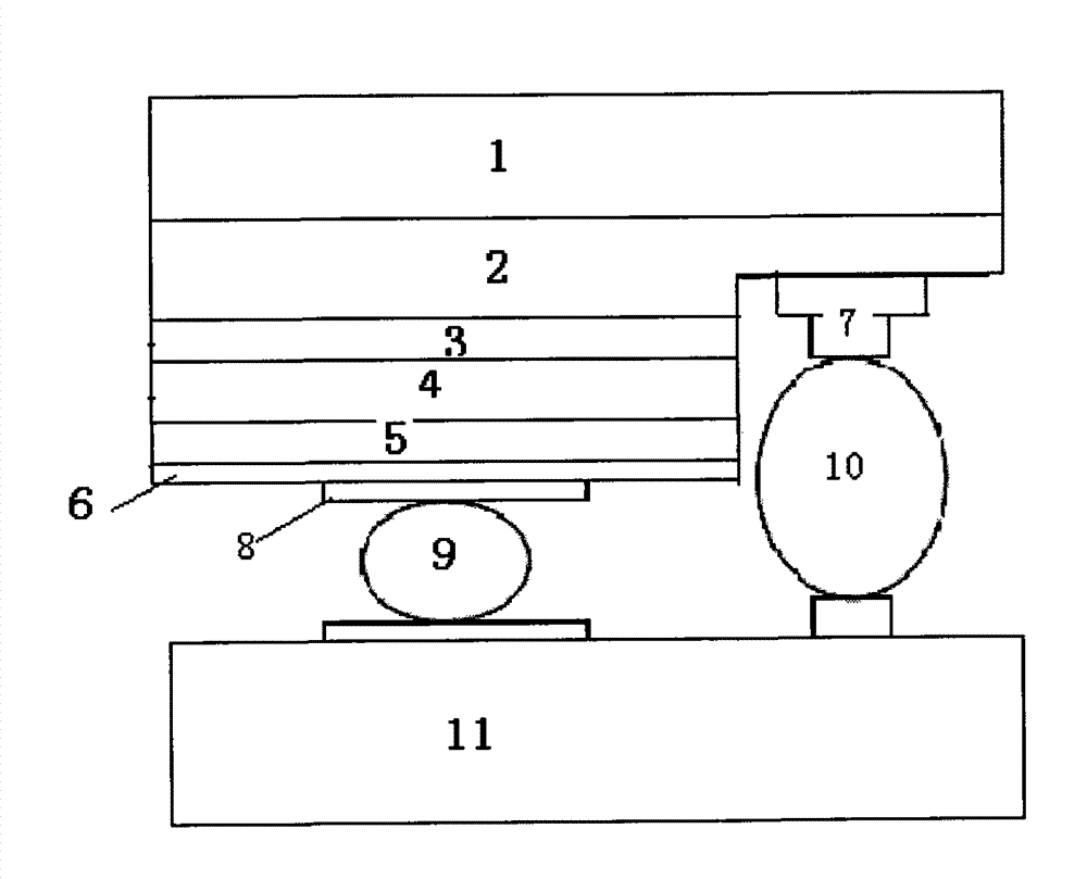
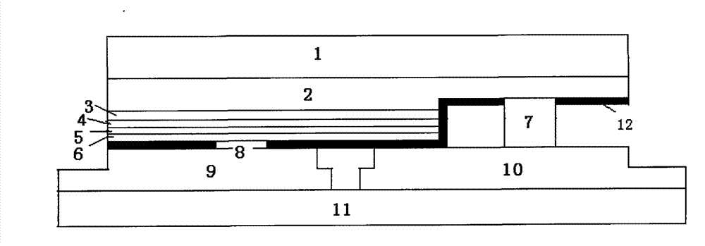
[0015] The structure of the flat panel flip-chip GaN-based LED of the present invention is figure 2 Improvements based on the flip-chip structure shown, such as image 3 with Figure 4 As shown, the light reflection layer 6 is etched with a step surface to the N-type GaN layer 4, an N electrode 7 is formed on the N-type GaN layer 4 of the step surface, and a P electrode 8 is formed on the light reflection layer 6. The outer ends of the N electrode 7 and the P electrode 8 are on the same horizontal plane. A layer of transparent insulating dielectric film 12 is plated on other areas on the surface where the P electrode pad and the N electrode pad are located except for the P electrode pad and the N electrode pad. A P welding plate 9 is made on the outer end of the P electrode solder joint, and an N welding plate 10 is made on the outer end of the N electrode solder joint. The P welding plate 9 and the N welding plate 10 are welded to the P electrode area and N of the thermally c...


PUM


Abstract

The invention provides a flat FCB (Flip Chip Bonding) GaN-based LED (Light-Emitting Diode) chip structure comprising a substrate. An N-type GaN layer, a QW (Quantum Well) active area, a P-type GaN layer, a current extension level and a light-reflecting layer are sequentially arranged below the substrate from top to bottom, a stepped surface to the N-type GaN layer is etched on the light-reflecting layer, an N electrode is made on the N-type GaN layer of the stepped surface, a P electrode is made on the light-reflecting layer and arranged on the same plane with the outer end of the P electrode, a transparent insulated medium film is coated on the plane of the P electrode bonding pad and the N electrode bonding pad except the regions of P electrode bonding pad and the N electrode bonding pad, a P bonding board is made at the outer end of the P electrode bonding spot, an N bonding board is made at the outer end of the bonding point of the N electrode, and the P bonding board and the N bonding board are bonded on a P electrode area and an N electrode area of a conductive Si or SiC substrate by cocrystallization or alloy. The insulated medium film is coated outside the PN bonding pads to prevent PN from being subjected to short circuits and a limit N-area electrode conductive flat is spliced to the P area desk.

Description

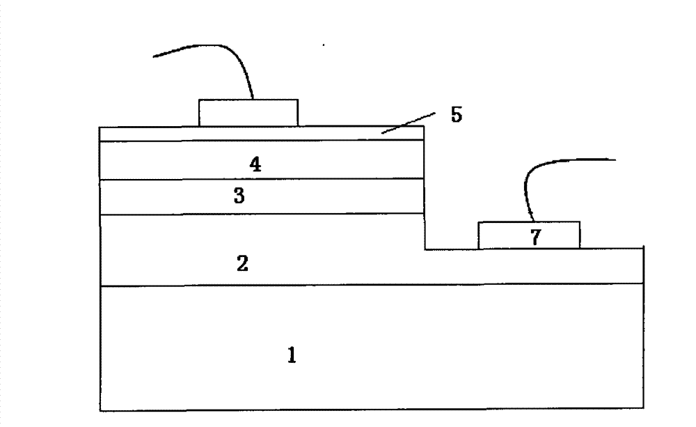
Technical field [0001] The invention relates to a GaN-based blue LED (light emitting diode) structure, which belongs to the technical field of light emitting diode structures. Background technique [0002] The structure of the traditional sapphire substrate GaN-based LED (light emitting diode) chip is as follows figure 1 As shown, an N-type GaN layer 2, a quantum well QW active region 3, a P-type GaN layer 4, and a current spreading layer 5 are arranged from bottom to top on the substrate 1, and an N electrode is arranged on the N-type GaN layer 2. 7. The electrode is just on the light-emitting surface of the chip. In this structure, a small portion of the P-type GaN layer 4 and the "light emitting" layer are etched to form electrical contact with the N-type GaN layer 2 below. Light is taken out from the upper P-type GaN layer 4. The limited conductivity of the P-type GaN layer 4 requires that another layer of current diffusion layer 5 be deposited on its surface. If the curr...

Claims


Application Information

Patent Timeline
Patent Type & Authority Patents(China)
IPC IPC(8): H01L33/62H01L33/44H01L33/64
CPCH01L2224/14H01L2224/49107
Inventor 沈燕徐现刚徐化勇郑鹏
Owner HUAWEI TEHCHNOLOGIES CO LTD
Learn More