Sputtering film forming method and sputtering film forming apparatus

A film forming method and sputtering technology, which is applied in sputtering plating, ion implantation plating, coating, etc., can solve problems such as difficulty in obtaining uniform film thickness, and achieve the effect of roughly uniform film thickness

Active Publication Date: 2010-10-13
ULVAC INC
View PDF2 Cites 6 Cited by
  • Summary
  • Abstract
  • Description
  • Claims
  • Application Information

AI Technical Summary

Problems solved by technology

[0008] Therefore, if Figure 11 As shown, even if two sets of magnetron cathodes are used, and the phase of the thin film shape formed by each magnetron cathode is shifted by half a cycle to form a film, although the deviation of the film thickness is improved compared with only one set of magnetron cathodes , but it is still difficult to obtain a uniform film thickness (refer to Figure 11 The single dotted line, the details will be described later)

Method used


Image

  • Sputtering film forming method and sputtering film forming apparatus
  • Sputtering film forming method and sputtering film forming apparatus
  • Sputtering film forming method and sputtering film forming apparatus

Examples


no. 1 approach

[0046] (Sputtering film forming device)

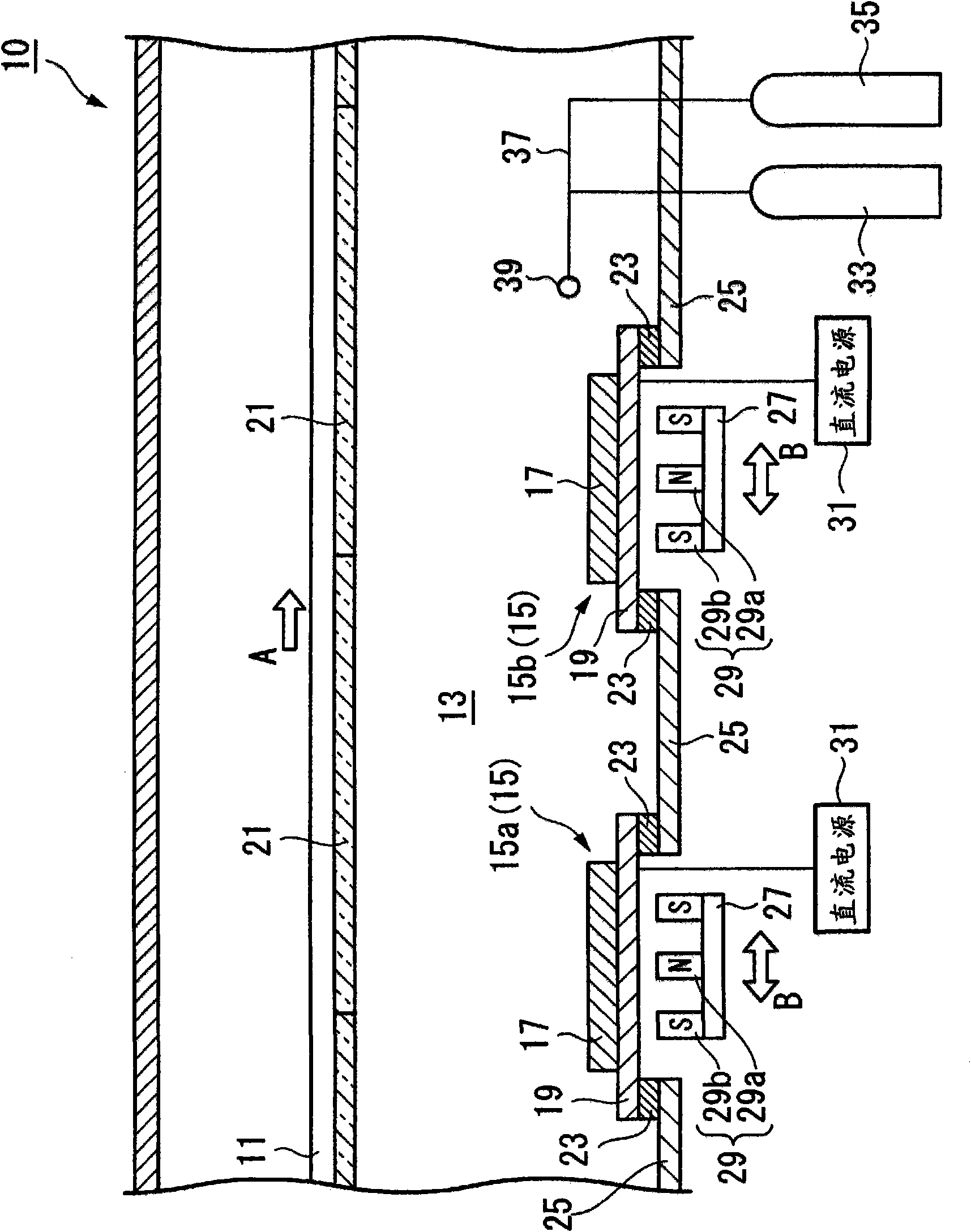
[0047] The following is based on Figure 1 to Figure 5 The sputtering film forming apparatus according to the first embodiment of the present invention will be described.

[0048] figure 1 It is a schematic configuration diagram (plan view) of the main part of the sputtering film deposition apparatus. Such as figure 1 As shown, the sputtering film forming device 10 is a mass-produced in-line sputtering device. In such a sputtering film forming apparatus 10 , substrates 21 are placed on a carrier 11 driven at a constant speed, and the substrates 21 are continuously and sequentially transported in the direction of arrow A (first direction) in the sputtering chamber 13 . As the conveyance method of the carrier 11 (substrate 21 ), a conveyance method such as a conveyance roller connected to a motor or a rack-and-pinion mechanism can be used. Alternatively, the upper edge and the lower edge of the substrate 21 may be sandwiched by gr...

no. 2 approach

[0088] Below, according to Figure 6 ~ Figure 8 A second embodiment of the present invention will be described.

[0089] In addition, since this embodiment differs from the first embodiment only in the arrangement structure of the magnetron cathodes, and other structures are substantially the same as the first embodiment, the same symbols are assigned to the same parts and detailed descriptions are omitted.

[0090] Image 6 It is a schematic configuration diagram (plan view) of the main part of the sputtering film deposition apparatus. Such as Image 6 As shown, the sputtering film forming device 110 is configured with three sets of magnetron cathodes 115 . In the magnetron cathode 115, the side where the substrate 21 first passes is set as the first magnetron cathode 115a, the second pass side is set as the second magnetron cathode 115b, and the third pass side is set as the third magnetron cathode 115b. control cathode 115c.

[0091] Here, the conveying speed of the su...

no. 3 approach

[0099] Below, according to Figure 4 , Figure 9 A third embodiment of the present invention will be described.

[0100] Since this embodiment differs from the second embodiment only in the moving speed of the permanent magnet of the magnetron cathode, and other structures are substantially the same as the second embodiment, the same symbols are assigned to the same parts and detailed description is omitted.

[0101] The sputtering film forming apparatus of this embodiment is substantially the same as that of the second embodiment. The sputtering film forming device 110 is equipped with three sets of magnetron cathodes 115 . In the magnetron cathode 115, the side where the substrate 21 first passes is set as the first magnetron cathode 115a, the second pass side is set as the second magnetron cathode 115b, and the third pass side is set as the third magnetron cathode 115b. control cathode 115c.

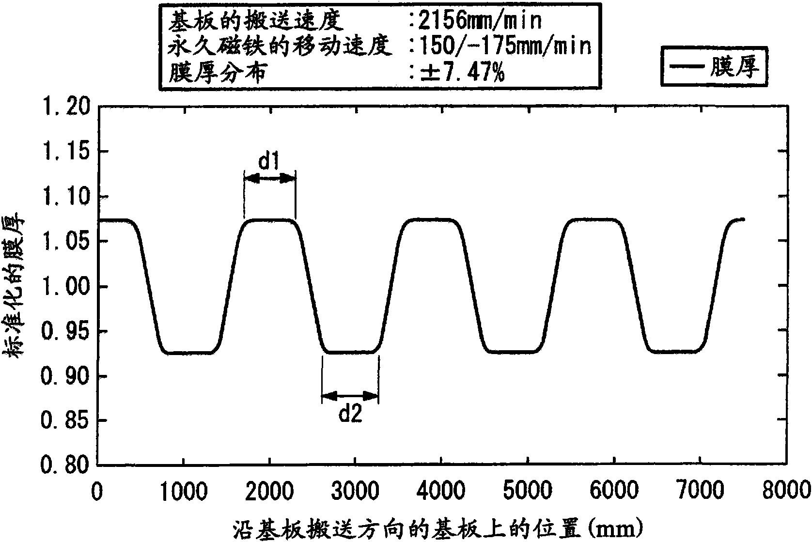
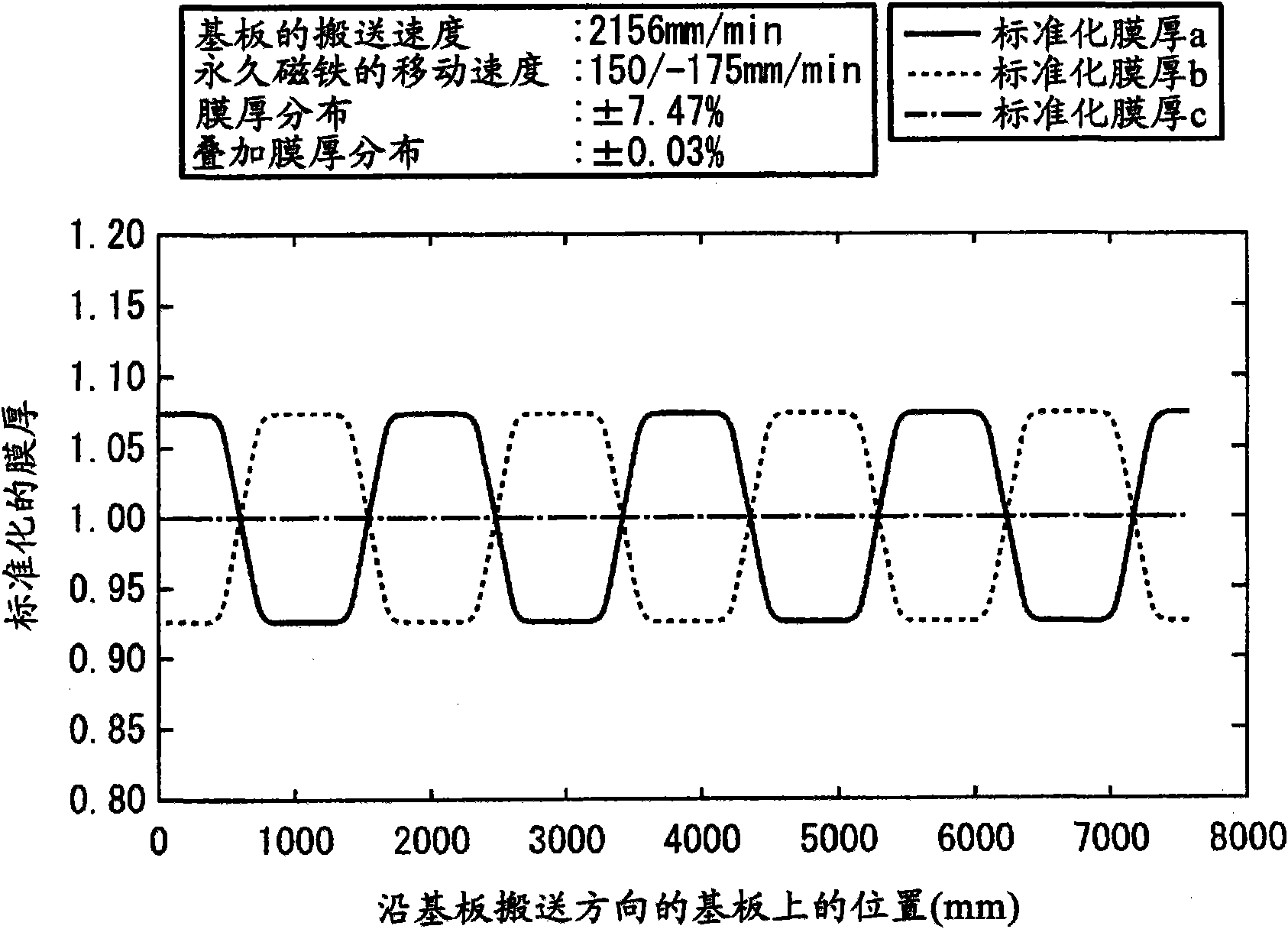
[0102] Here, the conveyance speed of the substrate 21 is set to 2156 mm / min. ...


PUM


Abstract

Provided is a sputtering film forming method wherein a film is formed on a substrate by sputtering by using a magnetron cathode having a magnet arranged on the rear side of a target, transferring the substrate in a first direction on the front side of the target, and reciprocating the magnet in the first direction and a second direction opposite to the first direction. A moving speed of the magnet in the first direction is permitted to be different from that in the second direction.

Description

technical field [0001] The invention relates to a sputtering film forming method and a sputtering film forming device. [0002] This application claims priority based on Japanese Patent Application No. 2008-010336 for which it applied in Japan on January 21, 2008, and uses the content here. Background technique [0003] Conventionally, when forming a thin film on a substrate by a sputtering method, a sputtering film forming apparatus using a magnetron cathode having a high deposition rate and excellent productivity has been widely used. In such a sputtering film forming apparatus, generally, a plurality of magnetron cathodes are arranged in a sputtering chamber along a substrate conveyance direction. Then, the substrate is conveyed facing the target of the magnetron cathode, and a thin film is formed on the surface of the substrate. [0004] Here, there is known a method of arranging a magnet on the back surface of a target, and forming a film while moving the magnet in or...

Claims


Application Information

Patent Timeline
Patent Type & Authority Applications(China)
IPC IPC(8): C23C14/35
CPCC23C14/542H01J37/3455H01J37/3408C23C14/352
Inventor 中村肇进藤孝明松田麻也子石野耕司
Owner ULVAC INC
Why Eureka
Try Eureka