Double side polishing device for wafer and double side polishing method

a polishing device and wafer technology, applied in the field of double side polishing devices for wafers and double side polishing methods, can solve the problems of affecting the polishing performance the change of the polishing ability and other factors of the polishing pad attached to the upper and lower turn tables, and the inability to maintain the quality of the wafer under varying polishing conditions, etc., to achieve excellent responsiveness in response, control the shape of the wa

Inactive Publication Date: 2005-06-09
SHIN-ETSU HANDOTAI CO LTD
View PDF10 Cites 33 Cited by
  • Summary
  • Abstract
  • Description
  • Claims
  • Application Information

AI Technical Summary

Benefits of technology

[0013] The present invention was conceived in light of the abovementioned problem. It is a first object of the present invention to provide a wafer double-side polishing apparatus and method in which it is possible to control wafer shape by deforming turn tables with excellent responsiveness in response to changes over time in polishing ability and other factors of polishing pads attributed to their life, clogging or other cause, and to polish the wafers stably with high precision without deteriorating wafer shape even in repeated polishing of a plurality of batches of wafers. Further, it is a second object of the present invention to provide a wafer double-side polishing apparatus and method that ensure good precision in wafer shape control by controlling the turn table shape with high precision and that ensure stable polishing with high precision even during repeated polishing of a plurality of batches of wafers.

Problems solved by technology

However, if a plurality of batches of wafers are polished repeatedly using a four-way double-side polishing apparatus as described above or double-side polishing apparatus that polishes wafers by causing the carrier plate to make a circular motion not accompanied by its rotation, the polishing ability and other factors of polishing pads attached to the upper and lower turn tables change over time due to polishing pads' life, clogging and other factors.
For this reason, polishing of a plurality of batches of wafers without replacement of the polishing pads has given rise to change in polished wafer shape over time with more polished batches, resulting in wafer shape differences between batches and problems that it is impossible to maintain wafer quality stably.
Although turn tables thought to be preferred for use in a double-side polishing apparatus are those that do not deform during wafer polishing, if such turn tables not deforming during wafer polishing are used, it will be difficult to ensure a fit between wafers and turn tables under varying polishing conditions.
Moreover, it will be impossible to control wafer shape in response to changes in polishing ability and other factors of polishing pads over time.
However, despite an attempt to control wafer shape by flowing cooling water, etc., through the turn tables and changing their temperature, the responsiveness of turn table deformation to varying turn table temperature (linearity relative to change in turn table temperature and the like) in conventional double-side polishing was poor, making it impossible to ensure high precision in the turn table shape control.
Particularly if polishing conditions and the like are substantially changed during wafer polishing, there was caused a problem that it has been impossible to control the turn tables into a desired shape through the temperature control in the turn tables alone.
When a plurality of batches of wafers are polished repeatedly, it has been difficult to control the turn table shape as desired with increasing number of wafer batches due to poor responsiveness of turn table deformation, making it impossible to control batch-by-batch wafer shape stably and with high precision.
In particular, repeated polishing of a plurality of batches of large-sized wafers such as 300 mm-diameter wafers has often led to a convex wafer shape, thus exhibiting remarkably deteriorations of a wafer shape such that flatness of GBIR (Global Back Ideal Range), etc. is deteriorated.
In other words, conventional turn table temperature control alone has failed to sufficiently control time-varying wafer shape.

Method used


Image

  • Double side polishing device for wafer and double side polishing method
  • Double side polishing device for wafer and double side polishing method
  • Double side polishing device for wafer and double side polishing method

Examples


example 1

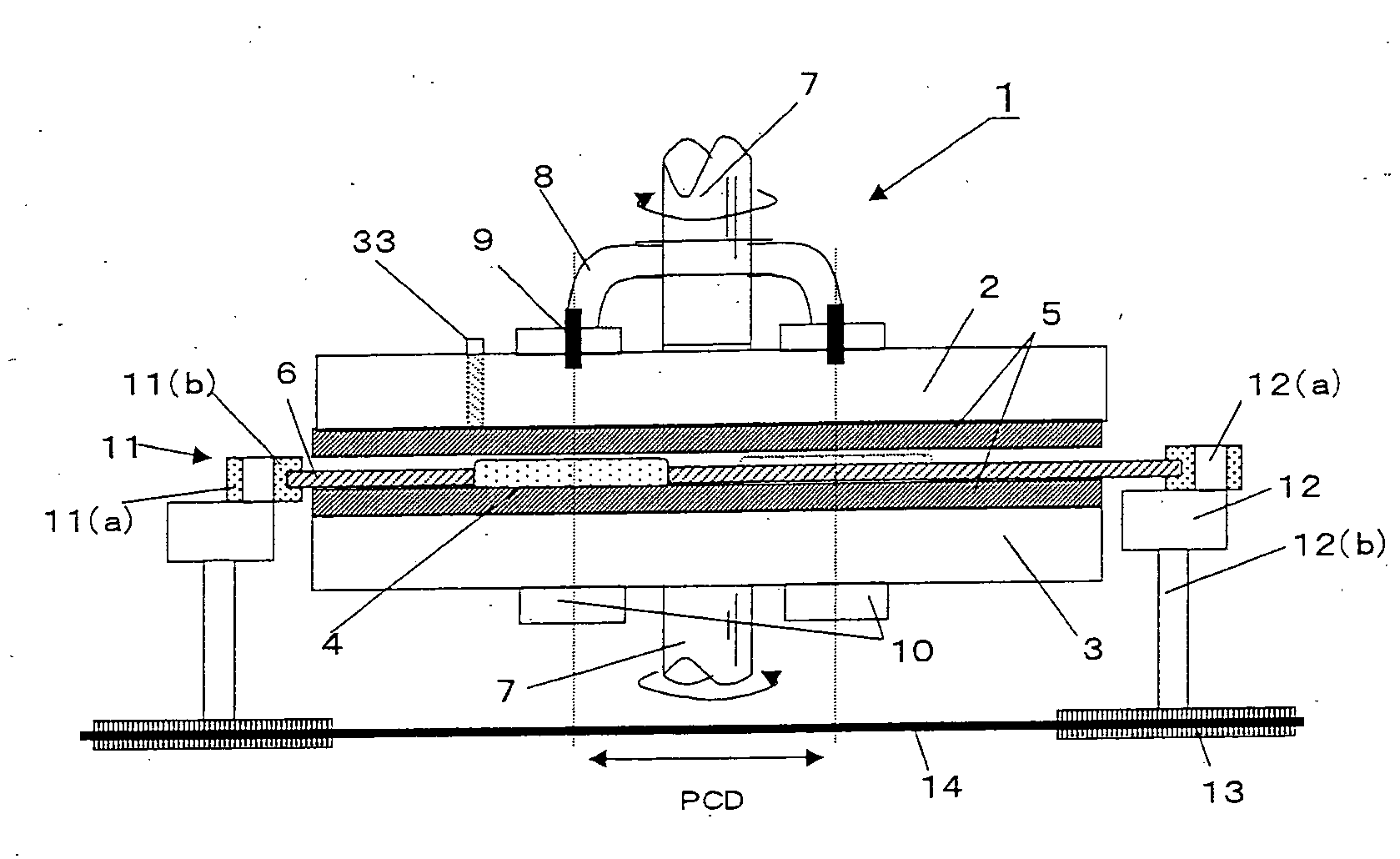
[0183] A double-side polishing apparatus was used in which the PCD of upper turn table load supporting points and the PCD of centers of the wafer holding holes on the carrier plate (centers of wafers held by the carrier plate) were coincident at 600 mm and in which the carrier plate performed a circular motion not accompanied by its rotation, with the average position of pitch circles formed by centers of wafer holding holes on the carrier plate coincident with the position of pitch circle formed by load supporting points of the upper turn table during polishing, as shown in FIG. 1.

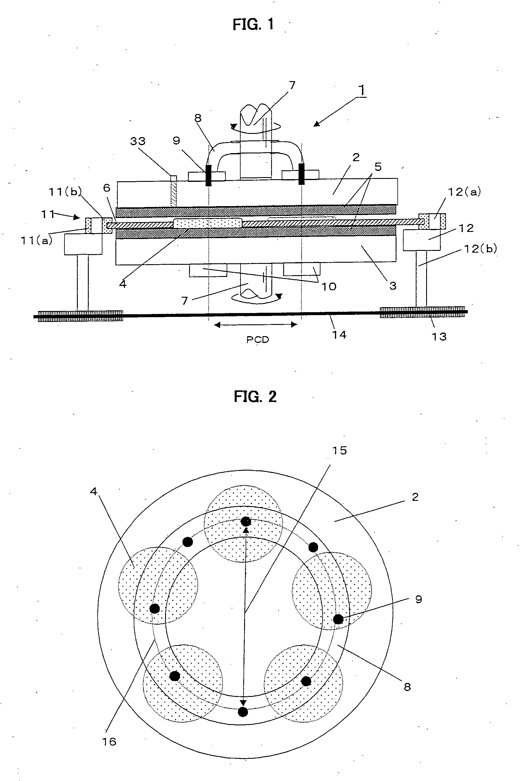
[0184] Using the double-side polishing apparatus, five silicon wafers having diameter of 300 mm (one batch) were first inserted into respective wafer holding holes of the carrier plate (carrier plate having five wafer holding holes) so as to be rotatable. Each wafer was pressed at 200 g / cm2 by the upper and lower turn tables to which soft non-woven cloths (polishing pads) were attached.

[0185] Then, the ...

example 4

[0199] Twenty batches of silicon wafers were repeatedly polished while controlling the turn table shape through adjustment of slurry supply amount using a wafer double-side polishing apparatus as shown in FIG. 9 in which the PCD of upper turn table load supporting points and the PCD of centers of the wafer holding holes on the carrier plate (centers of wafers held by the carrier plate) were both set to 600 mm and in which the carrier plate performed a circular motion not accompanied by its rotation, with the average position of pitch circles formed by centers of wafer holding holes on the carrier plate coincident with the position of pitch circle formed by load supporting points of the upper turn table during polishing.

[0200] Five silicon wafers having diameter of 300 mm (one batch) were inserted into respective wafer holding holes of the carrier plate (carrier plate having five wafer holding holes) so as to be rotatable. Each wafer was pressed at a pressing force of 200 g / cm2 by t...

example 6

[0206] Twenty batches of silicon wafers were repeatedly polished as example 6 while controlling the turn table shape through adjustment of slurry supply amount using a four-way wafer double-side polishing apparatus as shown in FIG. 11 in which the PCD of upper turn table load supporting points and the PCD of carrier plate centers were both set to 800 mm.

[0207] First, a total of 15 silicon wafers having diameter of 300 mm (one batch) were inserted into three wafer holding holes formed on each of the five carrier plates. Each wafer was polished with pressed at a pressing force of 200 g / cm2 by the upper and lower turn tables, to which soft non-woven cloths (polishing pads) were attached. The slurry used was that in which polishing abrasive grain consisting of colloidal silica of 0.05 μm in grain size was dispersed in alkali solution with pH 10.5. The initial slurry supply amount was set to 5.0 liters / min. In example 6, twenty batches of wafers were repeatedly polished without replacem...


PUM

PropertyMeasurementUnit
diametersaaaaaaaaaa
pHaaaaaaaaaa
diameteraaaaaaaaaa

Abstract

The present invention provides a wafer double-side polishing apparatus comprising at least a carrier plate having wafer holding holes; upper and lower turn tables to which polishing pads are attached; and a slurry supply means; with wafers held in the wafer holding holes, the carrier plate being moved between the upper and lower turn tables while supplying slurry, to simultaneously polish both front and back surfaces of wafers, wherein a PCD of upper turn table load supporting points that is a diameter of a circle joining load supporting points of the upper turn table coincides with a PCD of centers of the wafer holding holes on the carrier plate that is a diameter of a circle joining each center of the wafer holding holes on the carrier plate. Thereby, there can be provided a wafer double-side polishing apparatus and method in which it is possible to control wafer shape by deforming turn tables with excellent responsiveness, and to polish the wafers stably with high precision without deteriorating wafer shape.

Description

TECHNICAL FIELD [0001] The present invention relates generally to a polishing apparatus and a polishing method capable of maintaining time-varying wafer quality stably during wafer polishing using a double-side polishing apparatus, and more particularly to a wafer double-side polishing apparatus and a double-side polishing method for polishing wafers while controlling wafer shape by controlling at least an upper turn table shape of the double-side polishing apparatus that polishes both front and back surfaces of wafers at the same time. BACKGROUND ART [0002] A silicon wafer manufacturing method will be described as an example of conventional wafer manufacturing method. Silicon single crystal ingots are first grown by the Czochralski method (CZ method), etc., and sliced into silicon wafers. Then those silicon wafers are subjected to chamfering, lapping and etching steps in succession, after which the wafers undergo a polishing step where at least the wafer main surface is mirror-poli...

Claims


Application Information

Patent Timeline
Patent Type & Authority Applications(United States)
IPC IPC(8): B24B37/08H01L21/306
CPCH01L21/30625B24B37/08B24B37/04H01L21/304
Inventor TOMINAGA, HIROYOSHIHAYASHI, TOSHIYUKI
Owner SHIN-ETSU HANDOTAI CO LTD
Why Eureka
Try Eureka