Spread spectrum clock generating circuit with power-saving control

A technology for generating circuits and spreading spectrum, applied in the direction of delay line pulse generation, electrical components, pulse processing, etc., can solve the problems of not too high input clock signal frequency, high circuit cost, high circuit complexity, etc.

Inactive Publication Date: 2010-10-20
RAYDIUM SEMICON
View PDF0 Cites 5 Cited by
  • Summary
  • Abstract
  • Description
  • Claims
  • Application Information

AI Technical Summary

Problems solved by technology

The disadvantage of this well-known spread spectrum clock generator is that the circuit complexity is high and the circ

Method used


Image

  • Spread spectrum clock generating circuit with power-saving control
  • Spread spectrum clock generating circuit with power-saving control
  • Spread spectrum clock generating circuit with power-saving control

Examples


no. 1 example

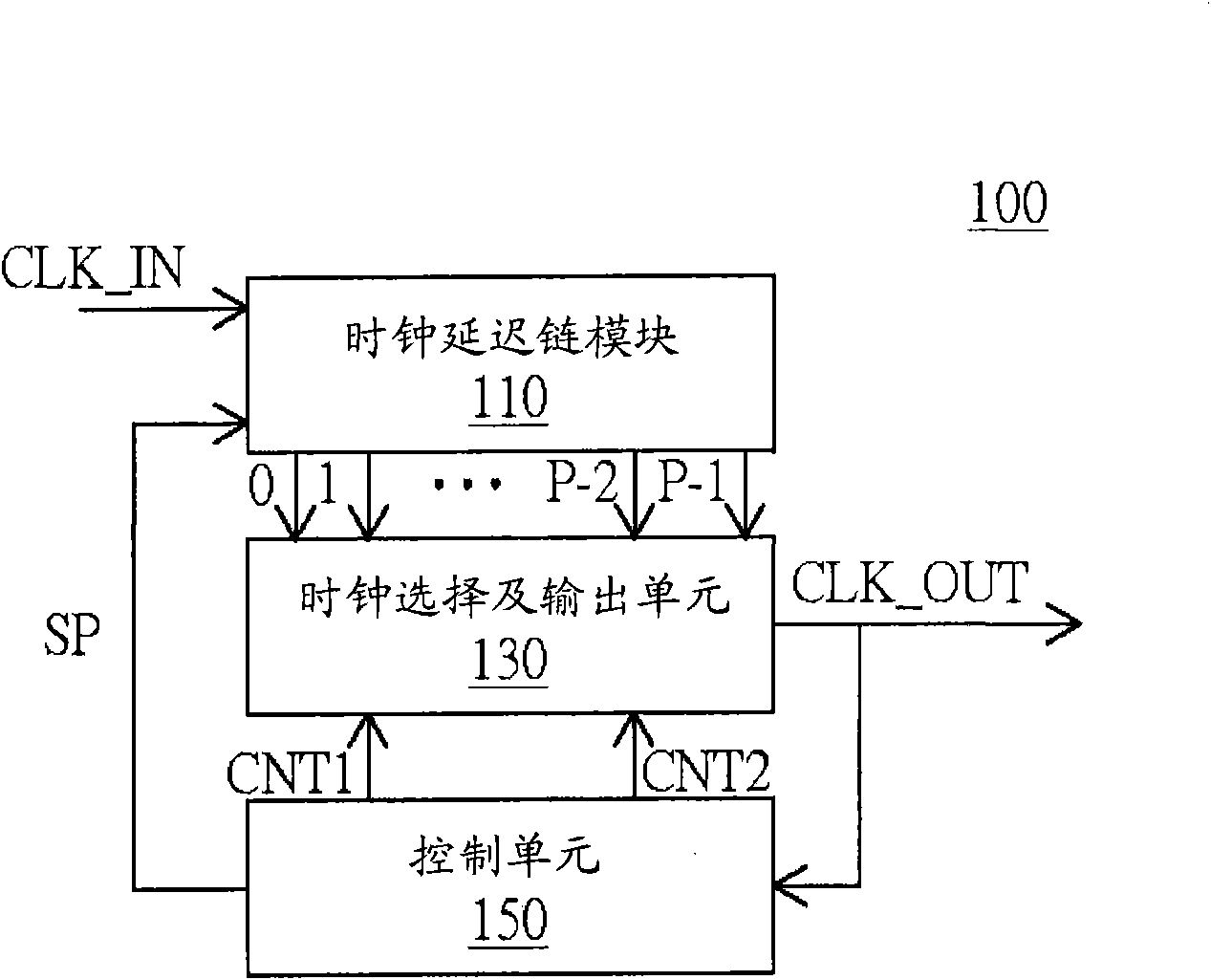
[0042] Please refer to figure 1 Shown is a block diagram of a clock signal spread spectrum generating circuit according to the first embodiment of the present invention. Such as figure 1 As shown, the clock spread frequency generating circuit 100 is used for spreading the input clock signal CLK_IN into the output clock signal CLK_OUT. The clock signal spread spectrum generation circuit 100 includes: a clock delay chain module 110 , a clock selection and output unit 130 and a control unit 150 .

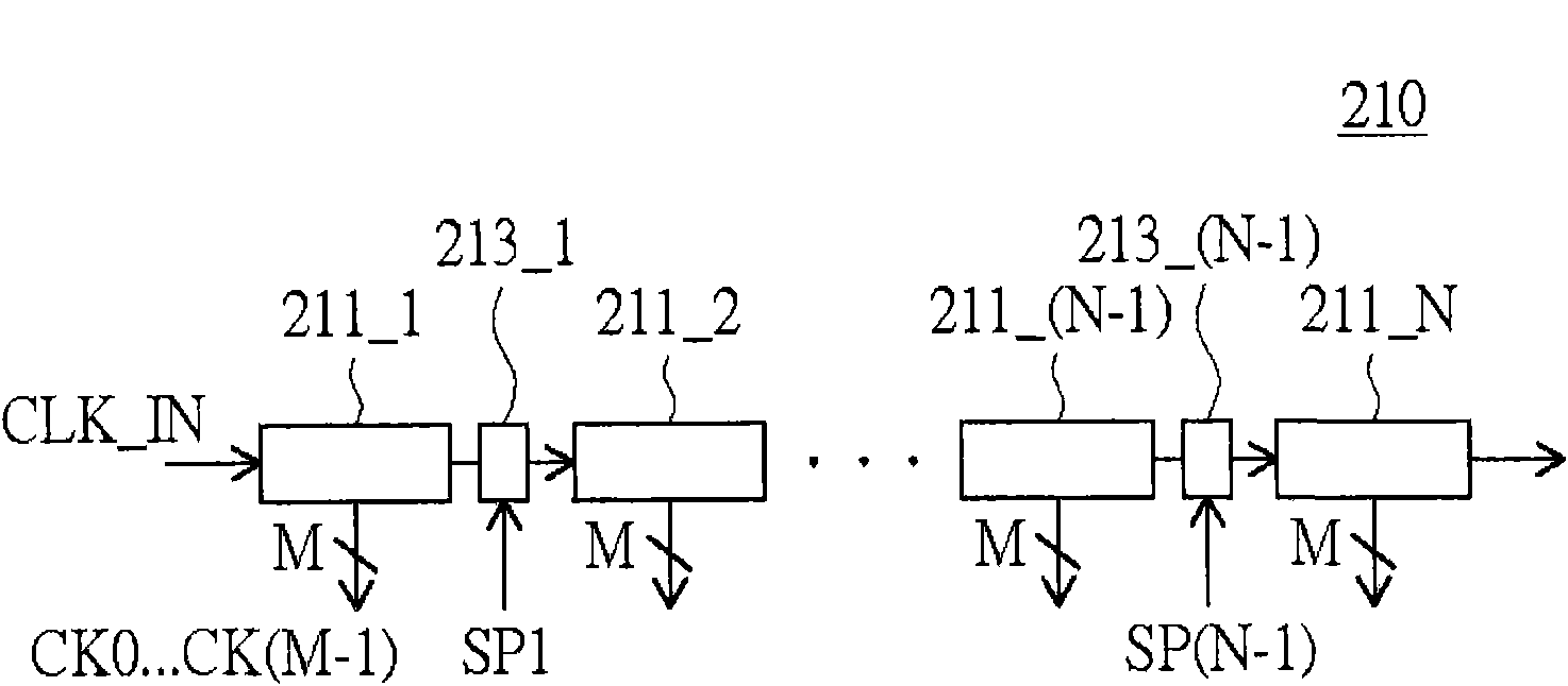
[0043] The clock delay chain module 110 is used for delaying the input clock signal CLK_IN to generate a delayed clock signal group including a plurality of delayed clock signals CK0 to CK(P−1), wherein P is a positive integer. The clock delay chain module 110 includes a plurality of clock delay chains (delay chain), for example figure 2 The clock delay chain module 210 shown includes: clock delay chains 211_1 to 211_N. Each clock delay chain includes a plurality of delay units (d...

no. 2 example

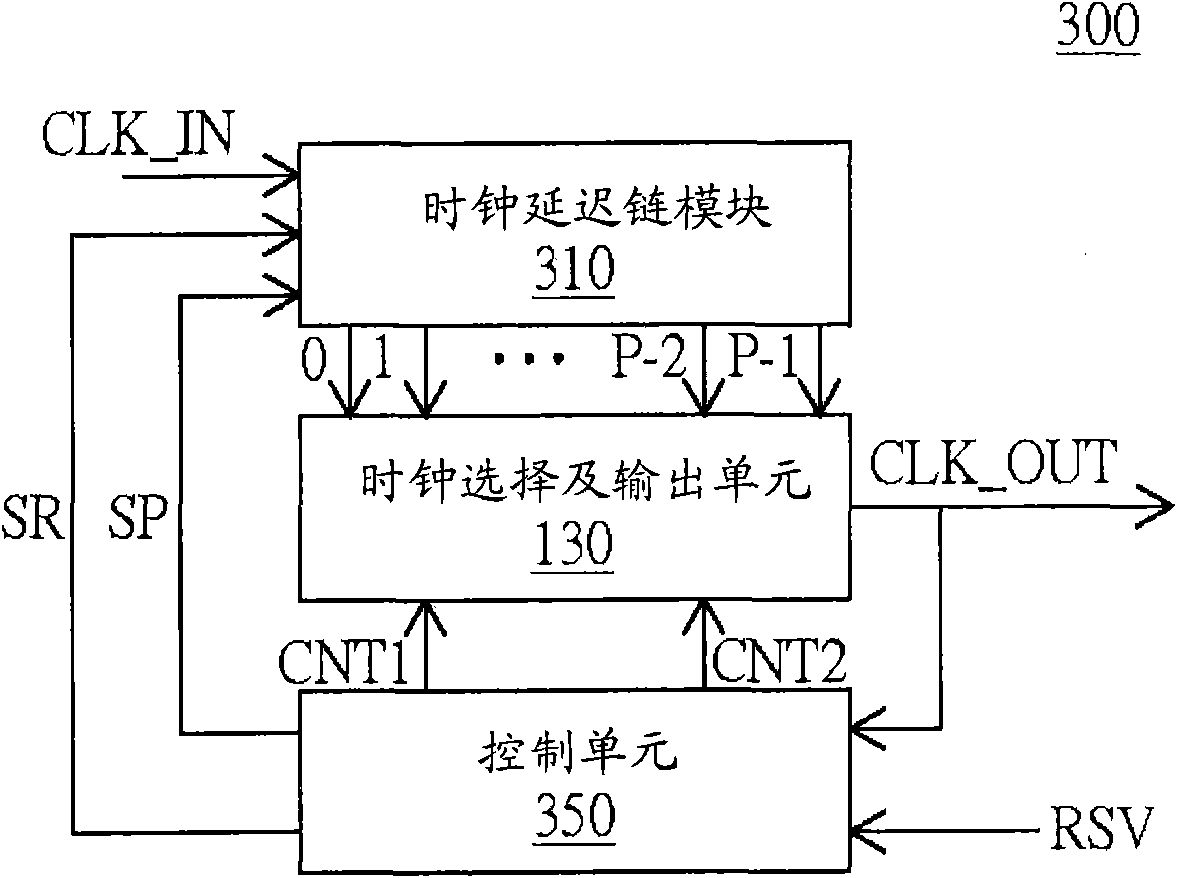
[0052] Please refer to image 3 The present invention further proposes a second embodiment of the clock signal spread spectrum generating circuit, which differs from the clock signal spread spectrum generating circuit 100 of the above-mentioned first embodiment in that the former also has a structure and an operation mode that can change the spread spectrum ratio. The following is image 3 In the description, the signals generated by the clock delay chain module 310 and the control unit 350 of the clock signal spread spectrum generation circuit 300 are described.

[0053] Such as Figure 4A Shown is an embodiment of the clock delay chain module 310 of the clock signal spread spectrum generating circuit 300 of the second embodiment. exist Figure 4A The clock delay chain module 410A in the figure 2 The difference of the middle clock delay chain module 210 is: the former also includes at least one selection unit 414 across non-adjacent clock delay chains, and at least two c...


PUM


Abstract

The invention provides a clock spread spectrum generating circuit with power-saving control, which is used for carrying out spread spectrum on the input clock signals into output clock signals. The spread spectrum clock generating circuit comprises a clock delay chain module, a clock selection and output unit and a control unit, wherein the clock delay chain module comprises a plurality of clock delay chains and is used for generating a plurality of delay clock signals; the control unit can generate a plurality of counter signals according to the output clock signals and can generate a plurality of power-saving control signals according to the counter signals; the clock selection and output unit is used for selectively combining the delay clock signals to generate output clock signals according to the counter signals; and the clock delay chain module is used for selectively starting the clock delay chains according to the power-saving control signals, therefore, spread spectrum output clock signals can be effectively generated and the purpose of energy saving can be achieved.

Description

technical field [0001] The invention relates to a spreading frequency clock generating circuit, and in particular to a spreading frequency clock generating circuit with power saving control. Background technique [0002] In order to meet various Electromagnetic Interference (EMI) regulations, spread spectrum clock technology has become a technology often used in the design of electronic systems. Its purpose is to reduce the peak energy in the electromagnetic spectrum generated by the system and make it distributed To a wider frequency band to make the electromagnetic spectrum of the electronic system comply with EMI regulations. [0003] Especially for portable devices, high-frequency clocks are often used and various components in the device need to be highly integrated. Relying on traditional methods of reducing EMI such as capacitors or metal shielding will not be sufficient to meet the portable design principles of portable devices and will increase a lot of cost. The ...

Claims


Application Information

Patent Timeline
IPC IPC(8): H03K3/86H03K5/13H03K5/135H03K5/14
Inventor 詹前煜谢宗轩
Owner RAYDIUM SEMICON
Why Eureka
Try Eureka