Method of fabricating an integrated CMOS-MEMS device

An oxide semiconductor and micro-electromechanical technology, which is applied in the field of MEMS device manufacturing, can solve problems such as substrate cracking and adhesive layer aging

Active Publication Date: 2010-10-27
TAIWAN SEMICON MFG CO LTD
View PDF6 Cites 9 Cited by
  • Summary
  • Abstract
  • Description
  • Claims
  • Application Information

AI Technical Summary

Problems solved by technology

Such handling can pose a risk of substrate cracking, glue line degradation, and / or other possible defects
Traditional approaches may require the use of etch stop layers when etching the backside of the substrate (e.g., bulk silicon micromachining) requires additional consideration of etch selectivity, post-etch surface roughness issues, and / or other potential issues

Method used


Image

  • Method of fabricating an integrated CMOS-MEMS device
  • Method of fabricating an integrated CMOS-MEMS device
  • Method of fabricating an integrated CMOS-MEMS device

Examples


Embodiment Construction

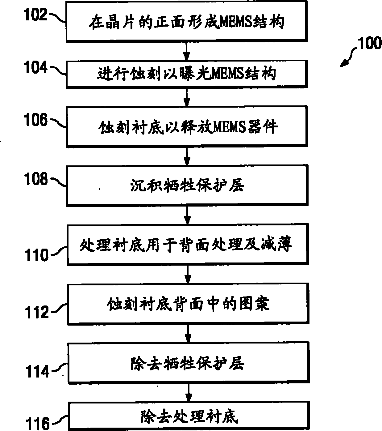
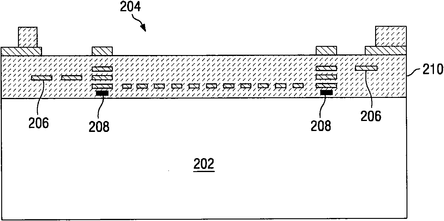
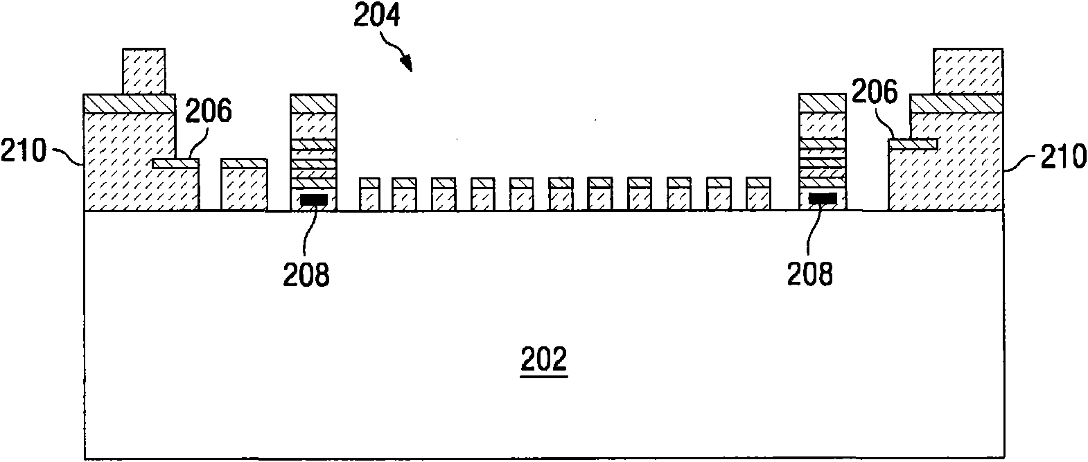
[0013] The present invention relates generally to the formation of MEMS devices, and more particularly to methods of forming MEMS devices on semiconductor substrates including CMOS circuits. However, it should be understood that the following provides many different embodiments or examples for implementing different configurations of the invention. The components and arrangements of specific examples are described below to simplify the present disclosure. Of course, these are just examples and not necessarily limited thereto. Furthermore, the present disclosure may repeat reference numerals and / or letters in different instances. These repetitions are for the purpose of simplicity and clarity, and furthermore, descriptions of a first layer being "on" a second layer, "overlying a second layer" (and similar descriptions) include instances where the first layer is in direct contact with the second layer. embodiments, and embodiments in which one or more layers are embedded betwe...


PUM


Abstract

An embodiment of a method is provided that includes providing a substrate having a frontside and a backside. A CMOS device is formed on the substrate. A MEMS device is also formed on the substrate. Forming the MEMS device includes forming a MEMS mechanical structure on the frontside of the substrate. The MEMS mechanical structure is then released. A protective layer is formed on the frontside of the substrate. The protective layer is disposed on the released MEMS mechanical structure (e.g., protects the MEMS structure). The backside of the substrate is processed while the protective layer is disposed on the MEMS mechanical structure.

Description

technical field [0001] The present invention relates generally to microelectromechanical systems (MEMS) technology, and more particularly to fabrication of MEMS devices using complementary metal-oxide-semiconductor (CMOS) compatible processes. Background technique [0002] With the benefits offered to integrating CMOS and MEMS devices onto a single substrate, such as system-on-chip (SOC) devices, various monolithic (eg, single substrate) CMOS-MEMS integration methods have been developed. This integration can provide lower parasitics (eg, resistance, inductance, and capacitance), lower cost, and / or increased performance. One approach developed for CMOS and MEMS device integration and processing involves forming CMOS devices and then forming MEMS devices using typical processing. In this approach, the backside of a substrate (eg, a wafer) is processed (eg, bulk silicon micromachining) followed by treatment of the front side of the substrate (eg, surface micromachining) during...

Claims


Application Information

Patent Timeline
Patent Type & Authority Applications(China)
IPC IPC(8): B81C1/00
CPCB81C2203/0728B81C2201/056B81C1/00246B81B2201/0257B81C2203/0714
Inventor 梁凯智吴华书彭利群黄琮诚刘醇明沈育民张华伦
Owner TAIWAN SEMICON MFG CO LTD
Why Eureka
Try Eureka