Connection hole test structure and method for preparing transmission electron microscopy

A technology for testing structure and connecting hole, which is applied in the field of testing structure of connecting hole and TEM sample preparation, which can solve the problem of inability to measure the thickness of the gluelayer and Barrierseed of the side wall of the connecting hole.

Inactive Publication Date: 2010-11-03
SEMICON MFG INT (SHANGHAI) CORP
View PDF1 Cites 5 Cited by
  • Summary
  • Abstract
  • Description
  • Claims
  • Application Information

AI Technical Summary

Problems solved by technology

[0004] The present invention solves the problem that the thickness of the Gluelayer and Barrier seed on the side wall of the co

Method used


Image

  • Connection hole test structure and method for preparing transmission electron microscopy
  • Connection hole test structure and method for preparing transmission electron microscopy
  • Connection hole test structure and method for preparing transmission electron microscopy

Examples


Embodiment Construction

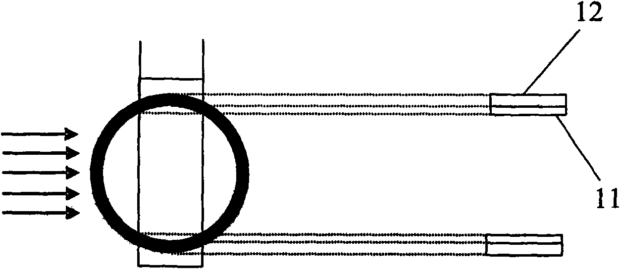
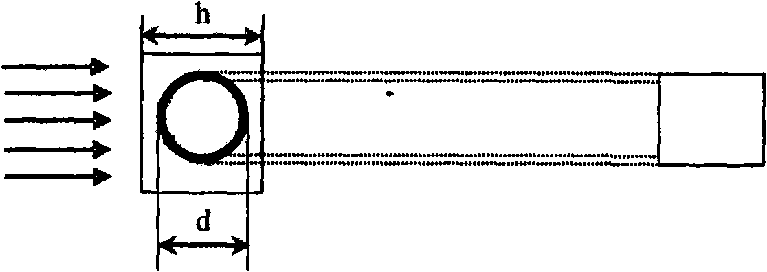
[0014] In view of the problems mentioned in the background technology, the embodiment of the present invention proposes that if the thickness of the structure used to measure the Gluelayer and Barrier seed in the connection hole test structure can be ensured to be greater than the thickness of the test sample, the above problems can be avoided. Based on this idea, the embodiment of the present invention proposes the following connection hole test structure to avoid the problem that the thickness of the connection hole Gluelayer and Barrier seed cannot be measured because the thickness of the connection hole is smaller than the thickness of the test sample.

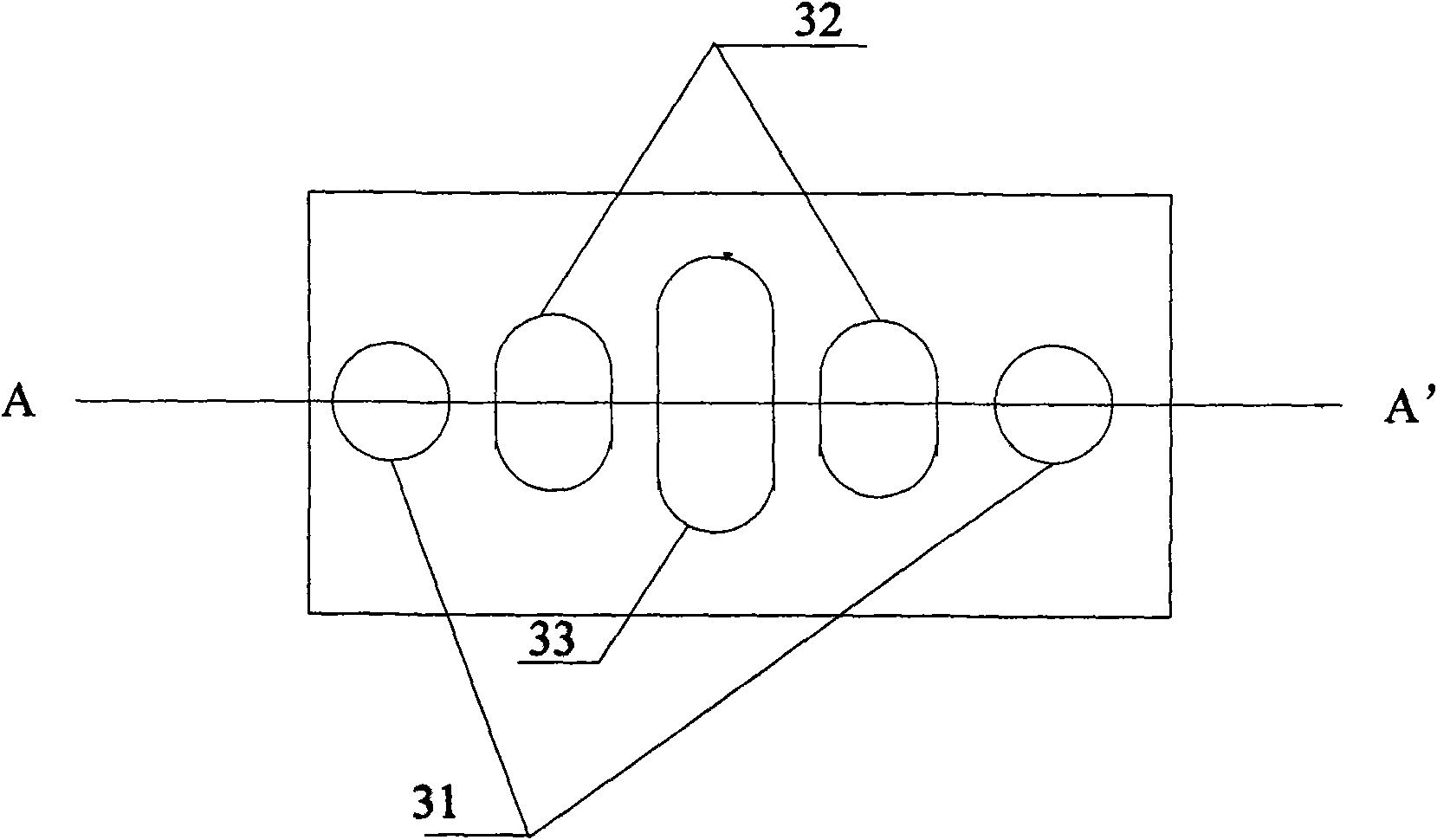
[0015] image 3 It is a top view of the connection hole test structure in the embodiment of the present invention. In combination with this figure, the connection hole test structure proposed in the embodiment of the present invention includes: the original hole 31, the calibration hole 32 and the measurement hole 33;

[0...


PUM


Abstract

The invention discloses a connection hole test structure and a method for preparing transmission electron microscopy (TEM), aiming at solving the problem that the side wall of the connection hole Glue Layer and the thickness of Barrier seed can not be measured in case that the diameter of the connection hole is less than the thickness of a detected sample wafer. The structure comprises a primary hole, a calibration hole and a measurement hole, wherein all the bottom surfaces of the primary hole, the calibration hole and the measurement hole are axis symmetric figures; a plane vertical to the bottom surface exists; a straight line of the plane, which is intersected with the bottom surfaces, is the symmetry axis of all the bottom surfaces; the primary hole is the connection hole; the thickness of the calibration hole perpendicular to the direction of the plane is the thickness of the detected sample wafer for controlling the thickness of the detected sample wafer to reach the predetermined thickness; the thickness of the measurement hole perpendicular to the direction of the plane is equal to the sum of the thickness of the calibration hole and the primary hole; the measurement hole is required to be identical to the object to be measured in the connection hole for measuring the size of the connection hole.

Description

technical field [0001] The invention relates to the field of integrated circuit manufacturing, in particular to a connection hole test structure and a TEM sample preparation method. Background technique [0002] The semiconductor manufacturing process is complex and the manufacturing cost is extremely high. In order to ensure the manufacturing quality, in the process of manufacturing semiconductor chips, test structures are usually manufactured on the wafer for testing after the manufacturing is completed. A semiconductor chip contains a lot of connection holes such as through holes (Via) and contact holes (CT), which have a significant impact on the quality of the semiconductor chip. At present, the industry generally manufactures a connection hole test structure in a semiconductor chip, and then uses the connection hole test structure to test the quality of the connection hole in the chip after the chip is manufactured. The connection holes are usually filled with fillers...

Claims


Application Information

Patent Timeline
IPC IPC(8): H01L23/544H01L23/522G01N1/28
Inventor 段淑卿庞凌华李剑李明
Owner SEMICON MFG INT (SHANGHAI) CORP
Why Eureka
Try Eureka