Packaging technology and packaging device of non-refrigerated infrared focal plane array device

A focal plane array and uncooled infrared technology, which is applied in the process of producing decorative surface effects, manufacturing microstructure devices, decorative arts, etc., can solve the problems of cumbersome process, complex structure, high cost, etc., and achieve the effect of reducing costs

Inactive Publication Date: 2010-11-24
UNIV OF ELECTRONICS SCI & TECH OF CHINA
View PDF4 Cites 20 Cited by
  • Summary
  • Abstract
  • Description
  • Claims
  • Application Information

AI Technical Summary

Problems solved by technology

The structure is complex, the proces...

Method used


Image

  • Packaging technology and packaging device of non-refrigerated infrared focal plane array device
  • Packaging technology and packaging device of non-refrigerated infrared focal plane array device
  • Packaging technology and packaging device of non-refrigerated infrared focal plane array device

Examples


preparation example Construction

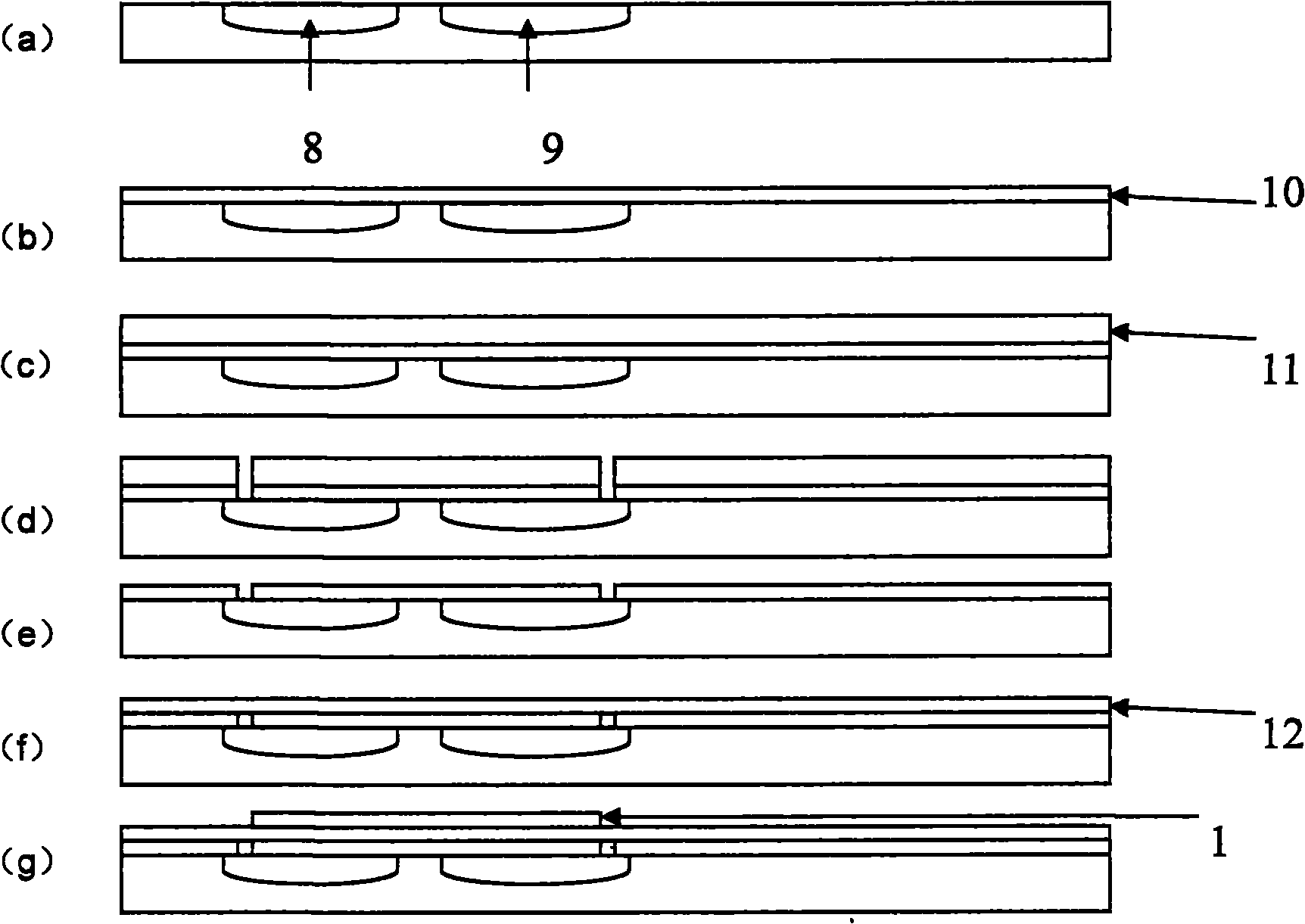
[0036] The preparation of the body is the most critical and complicated part of the process. In the field of packaging, it mainly includes three aspects: the semiconductor refrigerator, the negative temperature coefficient sensor, and the preparation of the welded metal frame.

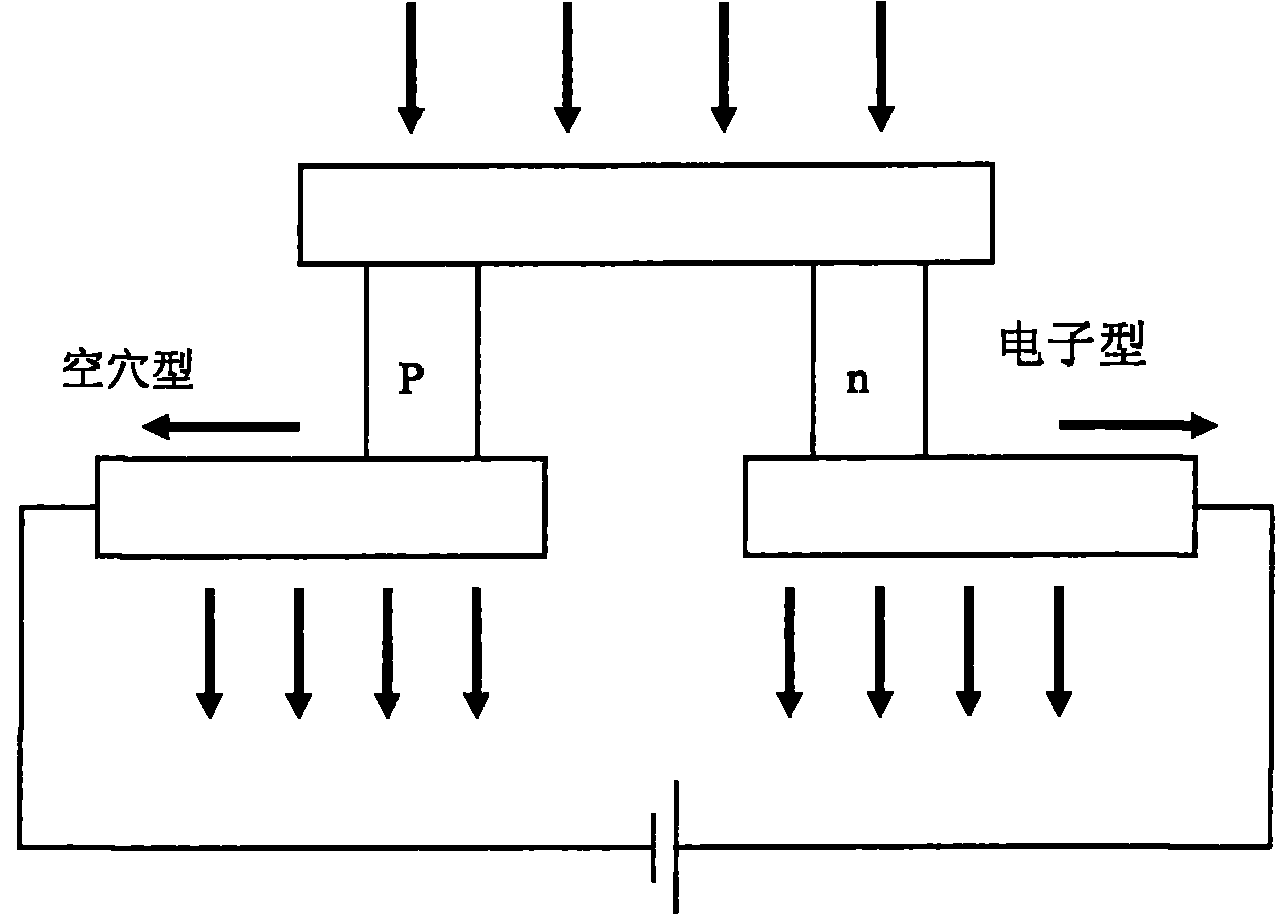
[0037] The semiconductor cooler is an integral part of the infrared focal plane, and its main function is to keep the temperature of the focal plane stable and the temperature distribution uniform. Its basic principle is to use the Peltier effect in semiconductors, such as figure 2 As shown, a galvanic pair is formed by welding an N-type and a P-type semiconductor particle with a metal connecting sheet. When the direct current flows from the N pole to the P pole, the upper end of the two will absorb heat, which is called the cold end, and the lower end will generate heat release, which is called the hot end. If the direction of the current is reversed, the hot and cold ends will switch to each other. ...

Embodiment 1

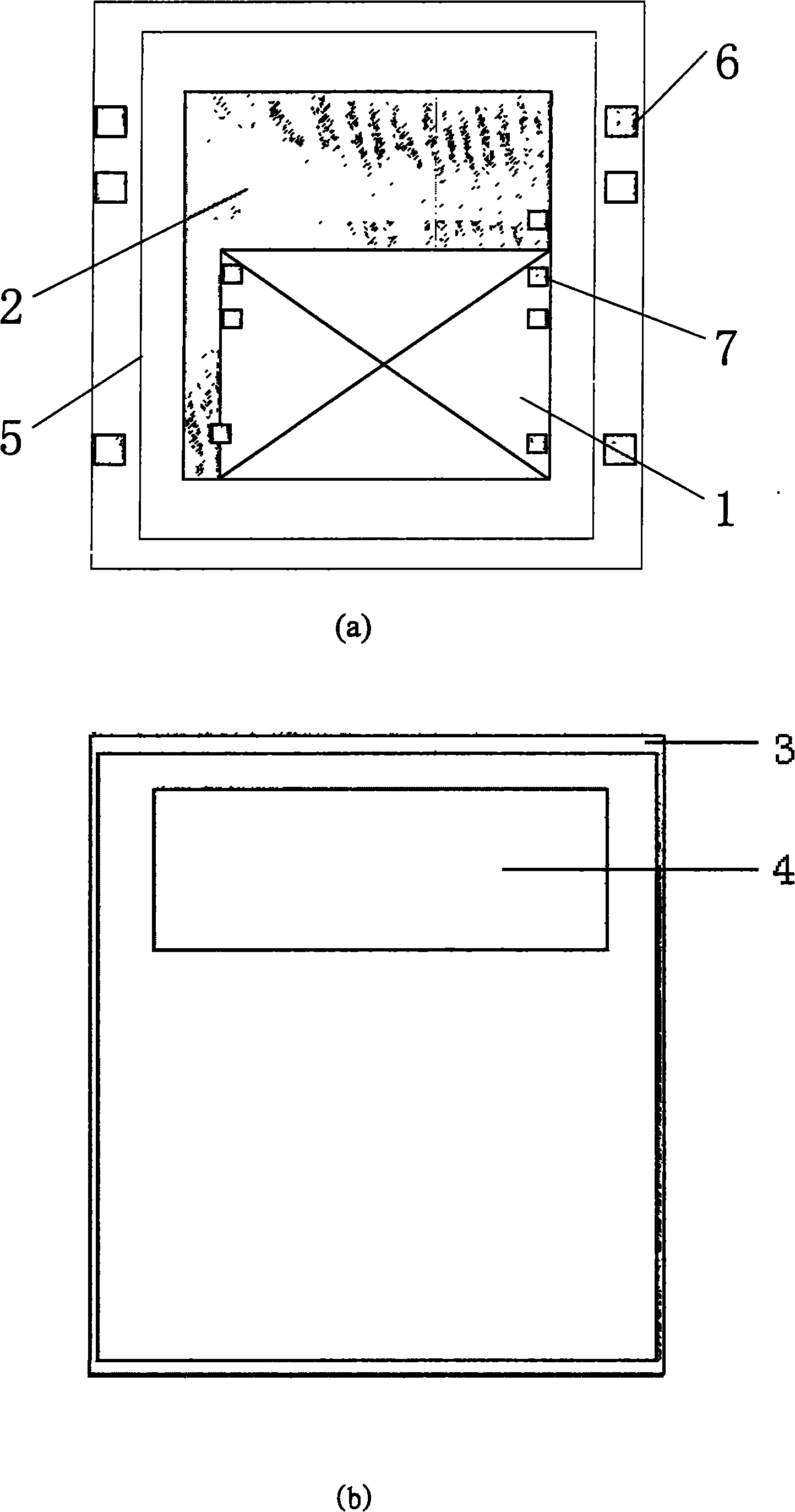
[0048] An uncooled infrared focal plane device, consisting of 320×240 uncooled infrared focal plane units, each uncooled infrared focal plane unit is 50um×50um in size, the array area is 16mm×12mm in size, and the integrated readout circuit is 22mm in size ×25mm, the readout method is the column gating method. Prepare 241 thermistors in the production, P, N injection according to 4mm×16mm, and 8mm×16mm specifications and connect with aluminum layer, the metal pattern is concentric with the chip, the size is 18mm×20mm. The cover area is 20mm×22mm.

Embodiment 2

[0050] An uncooled infrared focal plane device, consisting of 640×480 uncooled infrared focal plane units, each uncooled infrared focal plane unit is 15um×15um in size, the array area size is 9.6mm×7.2mm, integrated readout The size of the circuit is 15mm×18mm, and the readout method is the row strobe method. Prepare 641 thermistors in the production, P, N injection according to the specifications of 3.2mm×7.2mm, and 6.4mm×7.2mm and connect with aluminum layer, the middle gap is 50um, the metal pattern is concentric with the chip, and the size is 12mm×13mm. The cover size is 13mm×16mm.


PUM


Abstract

The invention discloses a packaging device of a non-refrigerated infrared focal plane array device and is characterized by comprising a body and a cover which are matched to work and are packaged into a whole by heating and tightly compression in a vacuum chamber, wherein (1) the body comprises a first substrate, the surface of the substrate is provided with a heavily doped region with P and N properties, the middle of the substrate is provided with a strip-shaped metal border, the upper part inside the strip-shaped metal border region is provided with a reading circuit region, a focal plane array region is arranged on the lower part, the area of the heavily doped region is larger than that of the focal plane array region which is provided with M*N units, a plurality of pressure welding discs are arranged between the strip-shaped metal pattern and the substrate edge, and a plurality of reference resistances are arranged in the focal plane array region; and (2) the cover comprises a second substrate, two sides of the second substrate are provided with diamond-like carbon films, any side of the second substrate is provided with a cover metal border corresponding to the strip-shaped metal border in the body, and a metal solder is arranged on the cover metal border.

Description

technical field [0001] The invention relates to the technical field of photoelectric packaging, in particular to the technical field of vacuum packaging for uncooled infrared detection. Background technique [0002] Electronic vacuum packaging is a major problem in controlling the cost of electronic devices. Traditional metal and ceramic packaging processes are complex and costly, and optoelectronic devices that need to work in vacuum conditions are also very expensive to test. The packaging form can utilize the existing microelectronic technology and greatly reduce the cost of the infrared vacuum device. [0003] With the development of integrated circuit and semiconductor process technology, the readout circuit of the uncooled infrared focal plane device is also integrated on a unified substrate. The device structure on the readout circuit of the microelectronics process has become a process trend in this field. After completing this type of process on a unified silicon w...

Claims


Application Information

Patent Timeline
IPC IPC(8): G01J5/02B81C1/00
Inventor 刘子骥蒋亚东李伟张杰郑兴
Owner UNIV OF ELECTRONICS SCI & TECH OF CHINA
Why Eureka
Try Eureka