Liquid crystal display panel and preparation method thereof
A technology of liquid crystal display panels and liquid crystals, applied in nonlinear optics, instruments, optics, etc., can solve problems affecting the display quality of liquid crystal display panels and gravity water ripples of liquid crystal display panels, so as to improve display effects and reduce high-temperature gravity water ripples and low-temperature air bubbles, reducing the effect of adverse phenomena
- Summary
- Abstract
- Description
- Claims
- Application Information
AI Technical Summary
Problems solved by technology
Method used
Image
Examples
no. 1 example
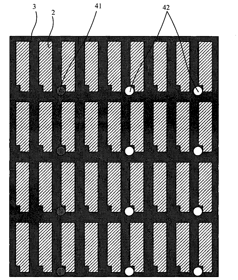
[0035] figure 1 It is a partial top view structure schematic diagram of a substrate in the liquid crystal display panel provided by the first embodiment of the present invention, figure 2 for figure 1 The schematic diagram of the side view structure, the spacer is arranged between the first substrate and the second substrate, figure 1 and 2 Shown is the case where the spacers are formed on one substrate, and specifically the color filter substrate. Such as figure 1 Shown is a top view of some pixel units on the color filter substrate. The color filter substrate usually includes a first base substrate 1 made of glass and other materials, and a color filter resin 2 and a black matrix 3 are arranged on the first base substrate 1 . Each resin block corresponds to a sub-pixel unit, and every three color filter resins 2 correspond to a pixel unit. The black matrix 3 corresponds to areas on the array substrate that need to be shielded from light, such as data scan lines, gate s...
no. 2 example
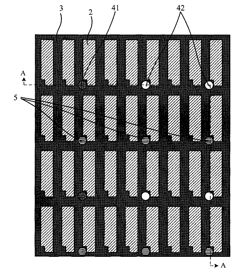
[0041] image 3 It is a partial top view structural schematic diagram of a substrate in a liquid crystal display panel provided by the second embodiment of the present invention, Figure 4 for image 3 The schematic diagram of the cross-sectional structure along the A-A line, the difference between this embodiment and the first embodiment is that the spacer in the above-mentioned first embodiment is the main spacer, and in this embodiment, the main spacer is placed between the two The distribution density between the substrates is lowered, and sub-spacers 5 are formed between the first and second substrates in addition to the first and second spacers 41 and 42 as main spacers. The sub-spacer 5 can also be arranged on the black matrix 3 of the color filter substrate, and when the liquid crystal is in a normal state, the height of the sub-spacer 5 is smaller than that of the main spacer. The so-called normal state of the liquid crystal refers to the state that the liquid cryst...
no. 3 example
[0045] Figure 5 It is a partial top view structure schematic diagram of a substrate in a liquid crystal display panel provided by the third embodiment of the present invention, Figure 6 for Figure 5 The difference between this embodiment and the above-mentioned first embodiment is that the spacer is made of three materials, that is, the third spacer 43 is also included, and the thermal expansion of the material used for the third spacer 43 The coefficient may be greater than, equal to, or less than the coefficient of thermal expansion of the liquid crystal. When the first spacer 41, the second spacer 42 and the third spacer 43 are present at the same time, the spacers of various materials are arranged at intervals, and it is preferable that the number ratio thereof satisfies the overall thermal expansion of the spacers The coefficient is approximately equal to the thermal expansion coefficient of the liquid crystal.
[0046] The specific number ratio can be calculated, a...
PUM
 Abstract
Description
Claims
Application Information


