Liquid crystal device, its mfg. method and electronic device

A technology of a liquid crystal device and a manufacturing method, applied in nonlinear optics, instruments, optics, etc., can solve the problems of substrate spacing deviation, contrast reduction, incomplete flatness, etc.

Inactive Publication Date: 2004-02-18
SEIKO EPSON CORP
View PDF1 Cites 4 Cited by
  • Summary
  • Abstract
  • Description
  • Claims
  • Application Information

AI Technical Summary

Problems solved by technology

[0005] However, in the manufacturing method of the above-mentioned liquid crystal device, although the liquid crystal is injected after the substrates are bonded, the liquid crystal injection process is a very troublesome process, and a simpler manufacturing method is desired.
In addition, in order to keep the distance between the substrates uniform, it is natural to provide a spacer between a pair of substrates, but the surface of the substrate is not completely flat after the formation of TFT elements, etc. deviation will occur
[0006] In addition, in the aforementioned Patent Document 1, the unevenness of the thickness of the liquid crystal layer is ±0.1 μm with respect to the thickness of the liquid crystal layer of 5 μm, that is, the unevenness of the thickness of the liquid crystal layer reaches ±2%.
Therefore, when such a liquid crystal device is applied to, for example, an STN-type liquid crystal device, a liquid crystal device using an active element, etc., the contrast will decrease, resulting in a decrease in display characteristics.
[0007] In addition, regarding the amount of spacers scattered in a liquid crystal device, if it is too large, a vacuum region may occur in the liquid crystal layer during storage at a low temperature, and if it is too small, there may be deviations in the distance between the substrates.

Method used


Image

  • Liquid crystal device, its mfg. method and electronic device
  • Liquid crystal device, its mfg. method and electronic device
  • Liquid crystal device, its mfg. method and electronic device

Examples


Embodiment 1

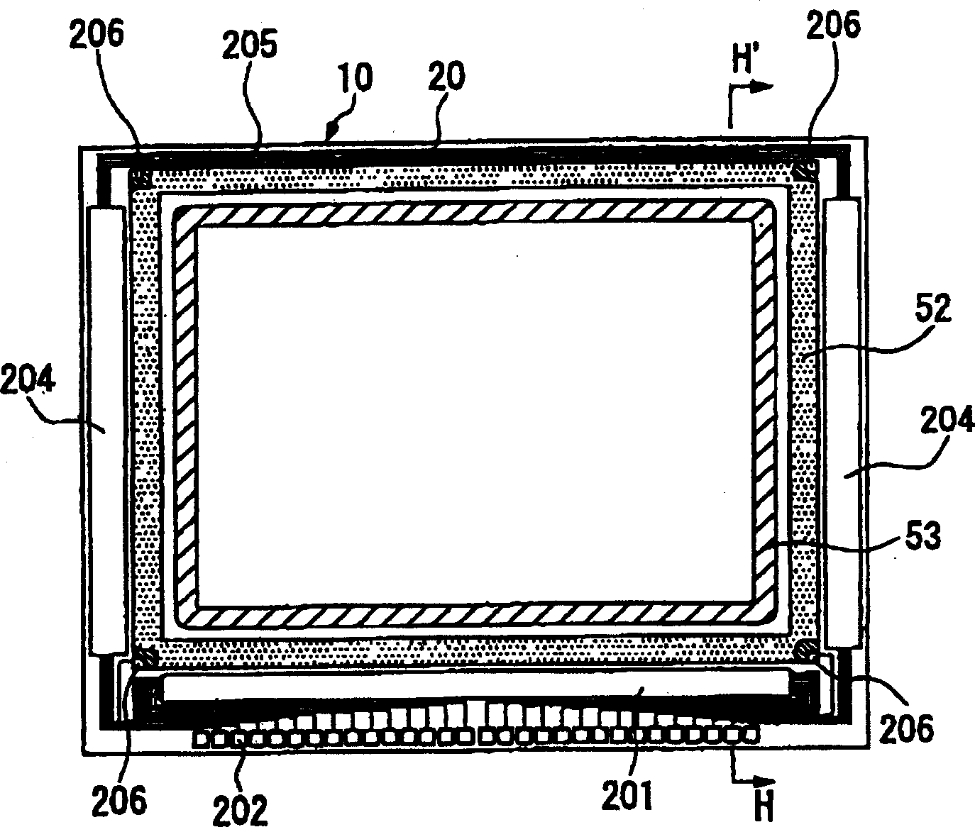
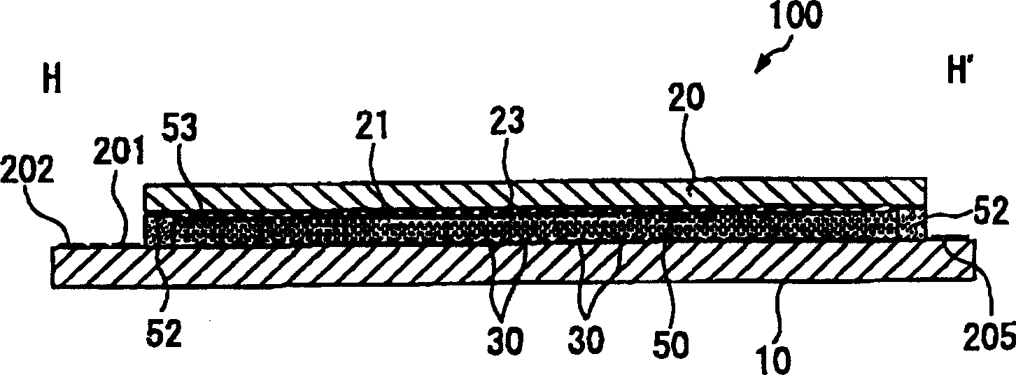
[0065] First, the liquid crystal display device of Example 1 used resin-made spacers 25 having an average particle diameter D=3 μm. Specifically, on a glass substrate (lower substrate) of 370mm×470mm, after using a dispenser, the above-mentioned adhesive was drawn in a closed frame shape, and as shown in Table 1, it was prepared at a density of 80 to 350 pieces / mm 2 The above-mentioned spacers were scattered and heated at 100° C. for 10 minutes to adhere the spacers to the surface of the substrate, and liquid crystal (super twisted nematic) was dropped using a dispenser.

[0066] Then, after attaching the substrate on which the liquid crystal was dropped and the other substrate (upper substrate) and releasing the atmosphere, use an output of 100mW / cm on the surface of the substrate 2 (365nm) high-pressure mercury lamp was used as a UV irradiator for UV irradiation. Next, heat in an oven to completely cure the adhesive. After such curing treatment, the liquid crystal panel is...

Embodiment 2

[0076] The average particle diameter of the spacers used was set at 6 μm, and the same liquid crystal device as in Example 1 above was produced, and the incidence of cell gap defects (Table 5), the incidence of vacuum regions at low temperatures (Table 6), and the occurrence of high-temperature voids were measured. Incidence of defective time box clearance (Table 7). In the same manner as in Example 1, ideal conditions were examined for these cell gap defect occurrence rates, low-temperature vacuum region occurrence rates, and high-temperature cell gap defect occurrence rates, and the measurement results are shown in Table 8. table 5 Table 6 Table 7 Table 8

[0077] From these results, it can be seen that regardless of the specific value of the average particle diameter D of the spacer, in relation to the layer thickness d of the liquid crystal layer, by setting the average particle diameter D and setting the density of the spacer under ideal conditions, the It is pos...


PUM

PropertyMeasurementUnit
particle sizeaaaaaaaaaa

Abstract

The invention provides a liquid crystal device in which the spacing between substrates in a plane of the substrate can be made uniform easily and simply, and which is less prone to producing a vacuum region in the liquid crystal layer at low temperatures by disposing spacers. A liquid crystal device has a pair of substrates (10, 20), spacers (25) located between the substrates (10, 20), and a liquid crystal layer (50) held between the substrates (10, 20). The liquid crystal (50) and spacers (25) are located inside a closed-frame-shaped seal material formed in a plane of the substrate, a density of the spacers (25) inside the seal material ranges from 100 to 300 / mm<2>, and the average particle size of spacers (25) D is set in the range of 0.96 d to 1.02 d, where a liquid crystal layer thickness in the region in which the spacers (25) are disposed is represented by d.

Description

technical field [0001] The present invention relates to a liquid crystal device, a method of manufacturing the liquid crystal device, and an electronic device having the liquid crystal device, and more particularly to a liquid crystal device having a spacer between substrates for keeping the thickness of the liquid crystal layer uniform. Background technique [0002] As a conventional liquid crystal device, there is a liquid crystal device in which a lower substrate and an upper substrate are bonded at respective peripheries with a sealing material, and a liquid crystal layer is sealed between the pair of substrates. At this time, a technique of disposing a spacer between a pair of substrates in order to make the interval between the substrates uniform within the substrate surface is well known. [0003] Such a liquid crystal device is manufactured by the following method. That is, after laminating and forming electrodes, an alignment film, etc. on the lower substrate and t...

Claims


Application Information

Patent Timeline
Patent Type & Authority Applications(China)
IPC IPC(8): G02F1/1339
CPCG02F1/13392G02F1/1339
Inventor 百濑洋一
Owner SEIKO EPSON CORP
Why Eureka
Try Eureka