Bonding pad, manufacturing method and bonding method thereof

A manufacturing method and bonding pad technology, which are used in semiconductor/solid-state device manufacturing, electrical components, electrical solid-state devices, etc. The effect of wire package failure

Active Publication Date: 2010-12-08
SEMICON MFG INT (SHANGHAI) CORP +1
View PDF1 Cites 10 Cited by
  • Summary
  • Abstract
  • Description
  • Claims
  • Application Information

AI Technical Summary

Problems solved by technology

The passivation layer made of these materials is relatively soft, and the bonding pad made of Al is also relatively soft, so when the first soldering of wire-bonded packaging is performed, the welding equipment will deform the bonding pad, resulting in wire-bonded packaging. Failure or degradation of wire bonded package quality

Method used


Image

  • Bonding pad, manufacturing method and bonding method thereof
  • Bonding pad, manufacturing method and bonding method thereof
  • Bonding pad, manufacturing method and bonding method thereof

Examples


Embodiment Construction

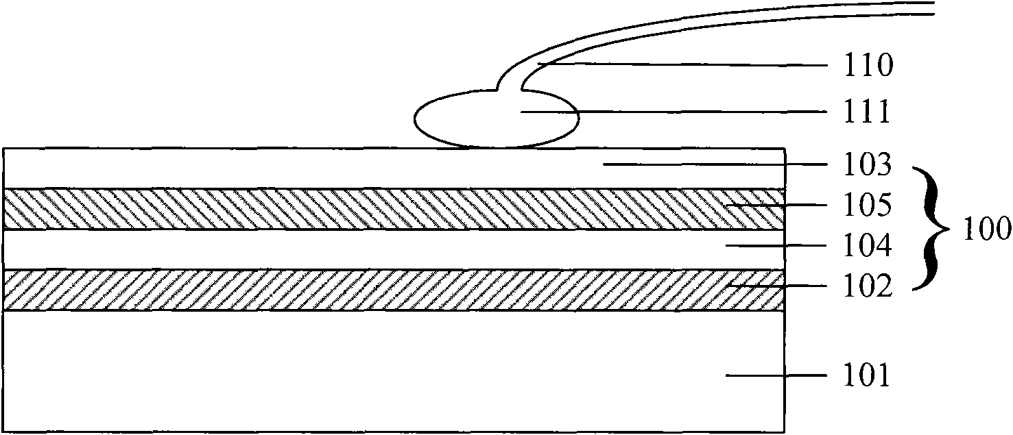
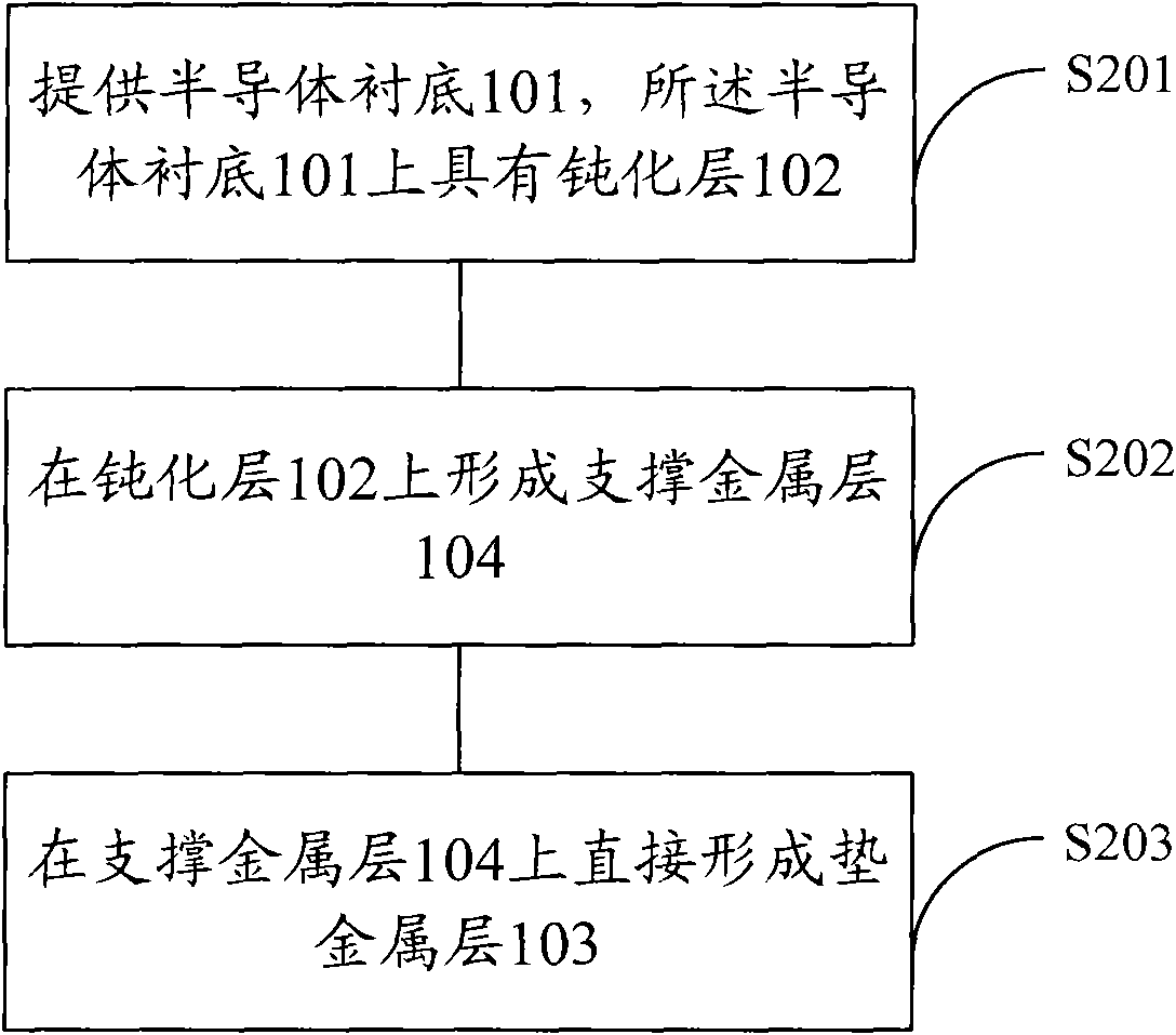
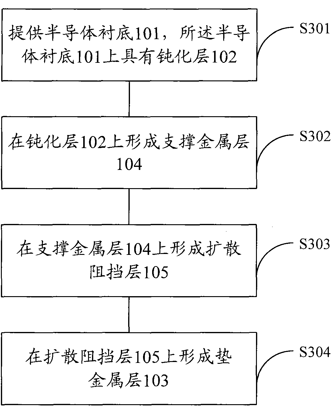
[0032] The inventors of the present invention found that in order to improve the hardness of the bonding pad and prevent the welding equipment from deforming the bonding pad during bonding, it is necessary to add an additional support metal layer with higher hardness to increase the hardness of the entire bonding pad. .

[0033] Therefore, if figure 1 As shown, the present invention provides a new bonding pad 100 for a semiconductor chip, which includes a passivation layer 102 on a semiconductor substrate 101 and a pad metal layer 103 on the passivation layer 102 . In addition, the bonding pad 100 further includes a support metal layer 104 disposed between the pad metal layer 103 and the passivation layer 102 .

[0034] Wherein, the pad metal layer 103 is used for direct bonding with the wire 110. In one embodiment of the present invention, the material of the wire 110 is Au. Correspondingly, the material of the pad metal layer 103 can be preferably bonded with Au. And lower...


PUM


Abstract

The invention relates to a bonding pad, a manufacturing method and a bonding method thereof. The bonding pad comprises a passivation layer and a pad metallic layer which are arranged on a semiconductor substrate, and a support metallic layer is arranged between the pad metallic layer and the passivation layer; and the support metallic layer is simultaneously used for rearrangement of wires, and adiffusion impervious layer is arranged between the pad metallic layer and the support metallic layer. Compared with the prior art, by introducing the support metallic layer between the passivation layer and the pad metallic layer, the invention overcomes the problem of failed wire bonding or lowered wire bonding quality caused by the softer passivation layer in the bonding pad in the prior art and avoids the problem of the increased cost resulted from that the material of the pad metallic layer is replaced by expensive metals.

Description

technical field [0001] The invention relates to the field of semiconductor manufacturing, in particular to a structure of a bonding pad, a manufacturing method thereof and a bonding method using the bonding pad. Background technique [0002] In the integrated circuit chip packaging process, an important process step is to electrically connect the bonding pads on the chip with the inner pins on the lead frame, and then transmit the electrical signals in the integrated circuit to the outside. This process step is called wire bonding in the art. [0003] The specific steps of wire bonding packaging are generally to use electronic image processing technology to determine the position of each contact on the chip and the contact on the inner pin corresponding to each contact after the lead frame is transferred from the magazine to the positioner, and then enter Wire bonding step. When welding wires, the contacts on the chip are used as the first solder joints, and the contacts o...

Claims


Application Information

Patent Timeline
Patent Type & Authority Applications(China)
IPC IPC(8): H01L23/485H01L21/60
CPCH01L24/48H01L24/03H01L2924/01082H01L2924/00014H01L2924/01079H01L24/05H01L2224/48463H01L2924/01033H01L2924/01327H01L2924/01029H01L2924/01074H01L2924/01022H01L2224/48091H01L2924/01013H01L2224/05554H01L2924/01024H01L2224/04042H01L2224/48H01L2924/14
Inventor 江卢山梅娜章国伟吴明峰
Owner SEMICON MFG INT (SHANGHAI) CORP
Why Eureka
Try Eureka