Grid pulse modulation circuit and shading modulation method thereof

A gate pulse modulation and voltage modulation circuit technology, applied in pulse shaping, static indicators, instruments, etc., can solve problems such as incomplete improvement and screen flickering, and achieve the effect of improving screen flickering.

Active Publication Date: 2010-12-15
AU OPTRONICS CORP
View PDF0 Cites 24 Cited by
  • Summary
  • Abstract
  • Description
  • Claims
  • Application Information

AI Technical Summary

Problems solved by technology

In the prior art, it utilizes the characteristics of forward conduction and reverse non-conduction of diode D0 to select an opportunity to transmit the power supply voltage AVDD to the output terminal 51 of the gate pulse modulation circuit 50, so as to control the lower limit of the chamfered voltage signal VGHM (corresponding to figure 2 The part enclosed by the dotted circle), however from figure 2 It can be found that the lower limit of the chamfered voltage signal VGHM is not a fixed value. One of the main reasons for the analysis is that the lower limit is affected by the conduction characteristics of the diode D0 itself. As a result, the flickering phenomenon of the screen has not been completely solved. improve

Method used


Image

  • Grid pulse modulation circuit and shading modulation method thereof
  • Grid pulse modulation circuit and shading modulation method thereof
  • Grid pulse modulation circuit and shading modulation method thereof

Examples


Embodiment Construction

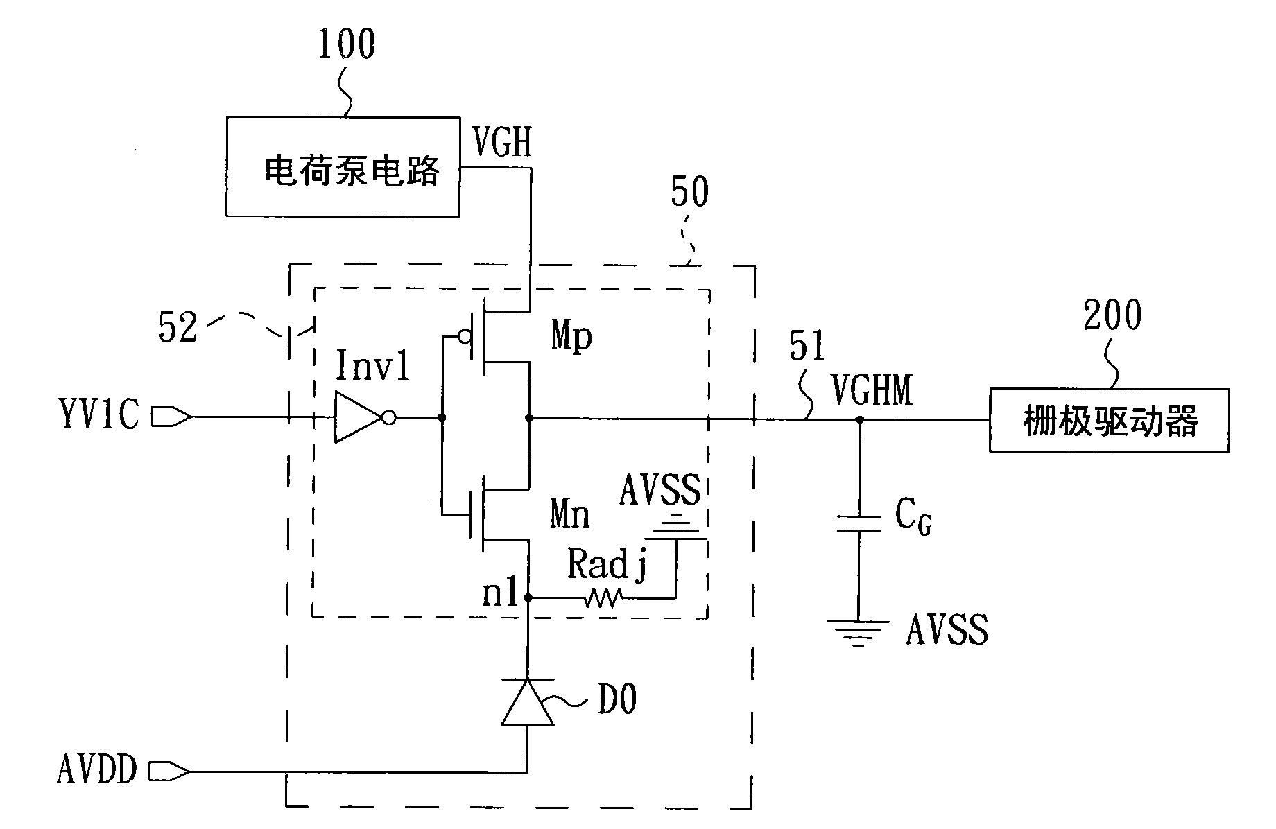
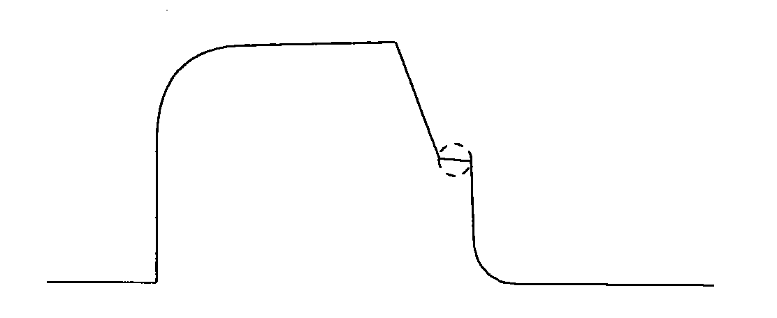
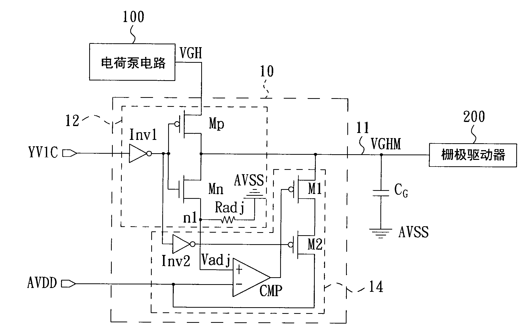
[0042] see image 3 , which shows a schematic diagram of the internal circuit structure of a gate pulse modulation circuit related to the first embodiment of the present invention.

[0043] Such as image 3 As shown, the gate pulse modulation circuit 10 is adapted to accept the control of the clipping control signal such as YV1C to generate a clipping voltage signal such as VGHM according to the gate power supply voltage such as VGH and a first preset voltage such as the supply voltage AVDD and pass the gate The output terminal 11 of the pole pulse modulating circuit 10 outputs a chamfered voltage signal VGHM to the gate driver 200 for the gate driver 200 to modulate the gate pulse. Here, the gate supply voltage VGH can be provided by the charge pump circuit 100, and the output terminal 11 of the gate pulse modulation circuit 10 is electrically coupled to the gate driver 200 and can pass through a ground capacitor C G Electrically coupled to a second preset voltage such as g...


PUM


Abstract

The invention relates to a grid pulse modulation circuit and a shading modulation method thereof. The grid pulse modulation circuit is provided with an output end, a voltage modulation circuit and a comparison control circuit, wherein the voltage modulation circuit is coupled between a grid power supply voltage and a second preset voltage and receives control of a shading control signal so as to shade and make the output end output a voltage signal for shading; the comparison control circuit comprises a comparator and a switch component; and the first input end of the comparator is coupled to a node of the voltage modulation circuit, while the second input end is coupled to a first preset voltage. When the voltage modulation circuit performs shading operation, the relative magnitude relation between the voltage at the node point and the first preset voltage decides the switching on and switching off states of the switch component so as to decide the occasion that the first preset voltage is transmitted to the output end.

Description

technical field [0001] The present invention relates to the field of display technology, and in particular to a gate pulse modulation circuit and an angle-cutting modulation method thereof. Background technique [0002] The driving method of the thin film transistor liquid crystal display (TFT-LCD) is to use the gate pulse signal to drive each pixel transistor to control the on and off state of each pixel; when a gate pulse signal is input to make the pixel transistor turn on, The data signal to be displayed will be transmitted to the pixel through the pixel transistor. If the pixel transistor is cut off, the data signal to be displayed will not be transmitted to the pixel through the pixel transistor. [0003] In the pixel array of the display panel, each pixel can be composed of equivalent resistance and equivalent capacitance. In this case, each gate pulse signal scan will cause the input waveform at the front end of the scan line to be different from that at the rear end...

Claims


Application Information

Patent Timeline
Patent Type & Authority Applications(China)
IPC IPC(8): H03K5/01G09G3/20G09G3/36
Inventor 张盟昇江佳璁
Owner AU OPTRONICS CORP
Why Eureka
Try Eureka