Multi-stack optical bandpass film with electro magnetic interference shielding for optical display filters

A multi-layer stacking, optical display technology, applied in the direction of filters, optics, optical components, etc., to achieve the effect of wide viewing angle and low transmittance

Inactive Publication Date: 2011-01-05
3M INNOVATIVE PROPERTIES CO
View PDF22 Cites 11 Cited by
  • Summary
  • Abstract
  • Description
  • Claims
  • Application Information

AI Technical Summary

Problems solved by technology

There is also a need for optical filters that are eas

Method used


Image

  • Multi-stack optical bandpass film with electro magnetic interference shielding for optical display filters
  • Multi-stack optical bandpass film with electro magnetic interference shielding for optical display filters
  • Multi-stack optical bandpass film with electro magnetic interference shielding for optical display filters

Examples


example

[0065] Optical analysis method

[0066] Measurements were performed on a Perkin Elmer Lambda 900 spectrophotometer equipped with a PELA-1000 integrating sphere attachment. The integrating sphere has a diameter of 150 mm (6 inches) and complies with ASTM methods E903, D1003, E308, etc., published in the third edition of "ASTM Standards on Color and Appearance Measurement," published by ASTM in 1991. The total light transmittance (TLT) of the sample is measured at the position on the front side of the sample, and the total light reflectance (TLR) of the sample is measured at the position on the back side of the sample. The incidence angles are normal (0°) and 70° for TLT and near normal (10°) and 70° for TLR. Measure front surface reflectance. Some of these samples were mounted on a 60mm x 80mm aluminum frame about 1mm thick to support them. Each frame has an fenestration measuring 50mm x 33mm. The membranes were adhered to these frames (bonded to the front of the membrane...

example 2 and 3

[0067] For Examples 2 and 3, near-normal TLR was measured with additional sample treatment to remove back surface reflections by grinding the back of the mounted film with 50 μm alumina powder in a shot peening cylinder and then spraying with black textured paint.

[0068] EMI shielding analysis method

[0069] All measurements were performed with an HP 8510 Vector Network Analyzer (HP 8510 Vector Network Analyzer from Hewlett Packard (Palo Alto, CA)) through a coaxial transmission cell (TEM cell), using a 10% span smoothing window, and all measurements complied with ASTM Method D4935. Results are reported in decibels (dB). Surface resistance was measured according to the eddy current method using a Model 717B Benchtop Conductance Monitor (available from Delcom Instruments Inc. (Prescott, WI.)).

[0070] Transmission Electron Microscopy (TEM) Analysis Method

[0071] TEM samples were prepared by room temperature ultrathin sectioning technique. Film samples were embedde...

example 1

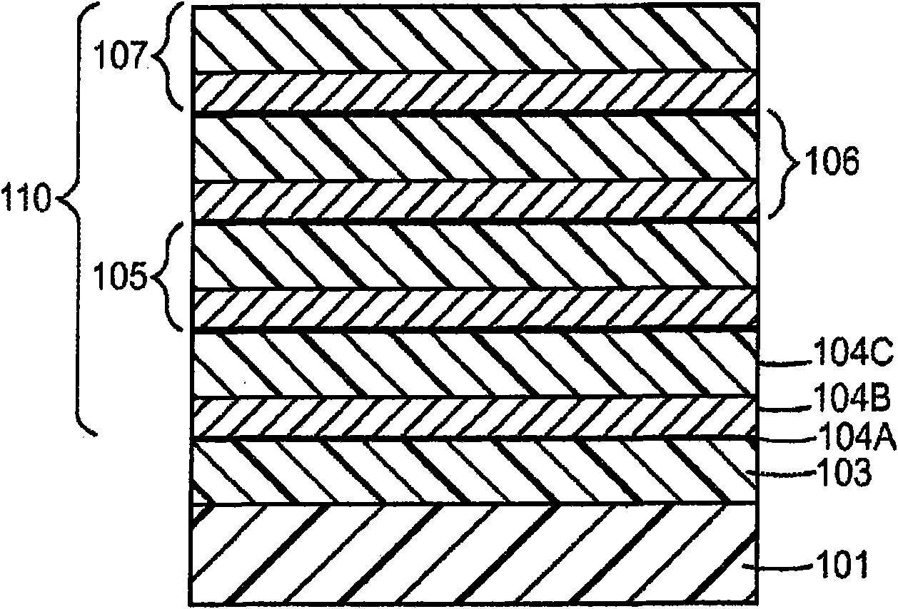
[0079] The substrate was TETORON XB-3 from DuPont Teijin Films. Using the manufacturing method described above, the operating conditions are listed in Table 1. Example 1 is a stacked optical filter with 4 dyads.

[0080] Table 1

[0081] Operating conditions of instance 1

[0082] frequency

Line speed

(m / min)

Plasma treatment (kW)

Seed Layer / Conductive Layer

polymer layer

1

18

Ti(N 2 )1kW

none

PTEA mixture

(1.36cm 3 / min, 91nm)

2

Rewind

none

none

none

3

18

Ti(N 2 )1kW

ZnO x (4kW) / silver (8kW,

15nm)

PTEA mixture

(1.10cm 3 / min, 71nm)

4

Rewind

none

none

none

5

18

Ti(N 2 )1kW

ZnO x (4kW) / Silver (8kW,

15nm)

PTEA mixture

(0.95cm 3 / min, 63nm)

6

Rewind

none

none

none

7

18

Ti(N 2 )1kW

ZnO x (4kW) / s...


PUM


Abstract

Provided are multi-component films useful as optical display filters. The optical display filters include a multi-layer stack that contains at least two dyads (106), i.e. pairs of layres including an electro-conducting layer (104B) and a dielectric space layer (104C), whereby in at least one of the dyads one transparent, organic layer with a refractive index greater than 1.49 is arranged. The filters have high visible light transmittance, low visible light reflection, and provide electromagnetic interference shielding in the range of 100-1000 MHZ.

Description

[0001] Related Patent Applications [0002] This patent application claims priority to US Provisional Application No. 60 / 983,781, filed October 30, 2007. technical field [0003] Multicomponent films useful as optical display filters are disclosed herein. Optical display filters are useful as components of active optical devices such as display panels, including plasma display panels. Background technique [0004] The use of electronic devices including flat panel displays is widespread and increasing at an increasing rate. These electronic devices include, for example, flat-panel displays, usually in the form of matrix displays, containing electroluminescent (EL) lamps, light-emitting diodes (LEDs), organic light-emitting diodes (OLEDs) or plasma components that generate visible radiation. Most of these displays require multiple optical filters to tune the display's performance characteristics, including neutrality and transmitted color levels, reflected radiant intensit...

Claims


Application Information

Patent Timeline
IPC IPC(8): G02B5/20G02B5/28
CPCG02B5/287
Inventor 克拉克·I·布莱特约翰·D·黎罗伯特·C·菲策尔史蒂芬·P·马基克里斯托弗·S·莱昂斯郑勋
Owner 3M INNOVATIVE PROPERTIES CO
Why Eureka
Try Eureka