Repairing structure and repairing method for liquid-crystal display (LCD) panel
A liquid crystal display panel and substrate technology, applied in nonlinear optics, instruments, optics, etc., can solve the problems of cost waste, inability to use laser cutting and repairing actions, display panels can only be scrapped, etc., and achieve the effect of reducing costs
- Summary
- Abstract
- Description
- Claims
- Application Information
AI Technical Summary
Problems solved by technology
Method used
Image
Examples
Embodiment Construction
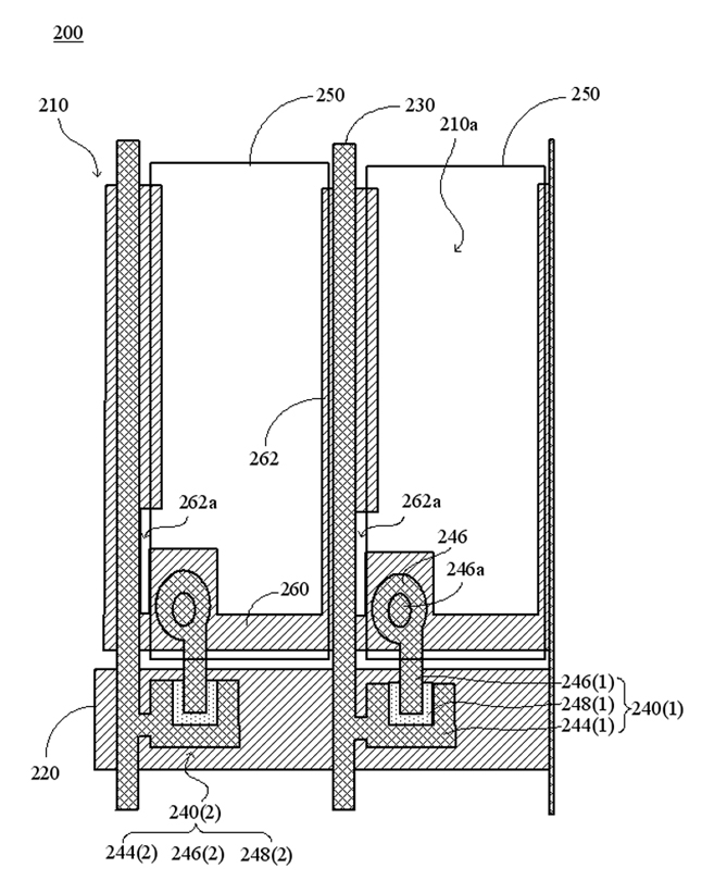
[0048] A preferred embodiment of the present invention will be described in detail with the accompanying drawings and the following description. In different drawings, the same reference numerals represent the same or similar components. image 3 A top view showing the repair structure of the liquid crystal display panel according to the preferred embodiment of the present invention. Please refer to image 3 The repair structure of the liquid crystal display panel 200 in this preferred embodiment is described with two adjacent pixel structures, which include a substrate 210, a plurality of scanning lines 220, a plurality of signal lines 230, a plurality of thin film transistors (Thin Film Transistor, TFT) 240 , a plurality of pixel electrodes (Pixel electrode) 250 , and a plurality of shared wires 260 .
[0049] The scan lines 220 are arranged in parallel on the substrate 210 , and the signal lines 230 and the scan lines 220 are alternately arranged and separated from each ot...
PUM
 Abstract
Description
Claims
Application Information


