A voltage level shifter

一种电压电平移位、电压域的技术,应用在使用介电元件的逻辑电路、电气元件、逻辑电路等方向,能够解决逻辑弱化、单一NWELL电压移位器不可用等问题

Inactive Publication Date: 2011-01-12
ARM LTD
View PDF2 Cites 11 Cited by
  • Summary
  • Abstract
  • Description
  • Claims
  • Application Information

AI Technical Summary

Problems solved by technology

Due to this instability, figure 2 The single NWELL voltage shifter is not available in standard cell libraries for deep submicron technology
Also, in the so-called "FF corner" corresponding to fast NMOS and fast PMOS transistors and high temperature corners where leakage current may be high, even if the logic input is 0, due to the the high resistance path, figure 2 The potential of node 250 may become non-zero
As a result, PMOS transistor 212 may enter a "triode region" (i.e., a linear region) that would weaken the logic of node 252 at the output of circuit 200.

Method used


Image

  • A voltage level shifter
  • A voltage level shifter
  • A voltage level shifter

Examples


Embodiment Construction

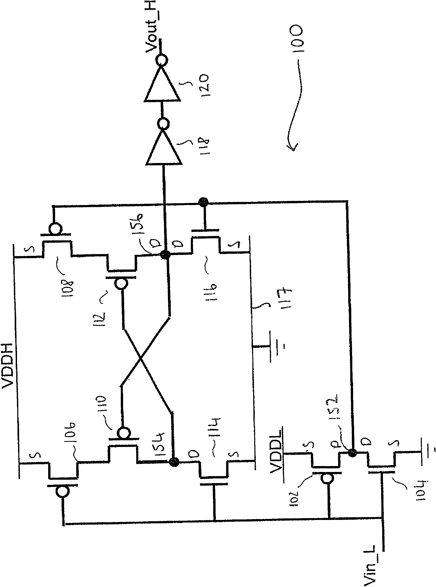
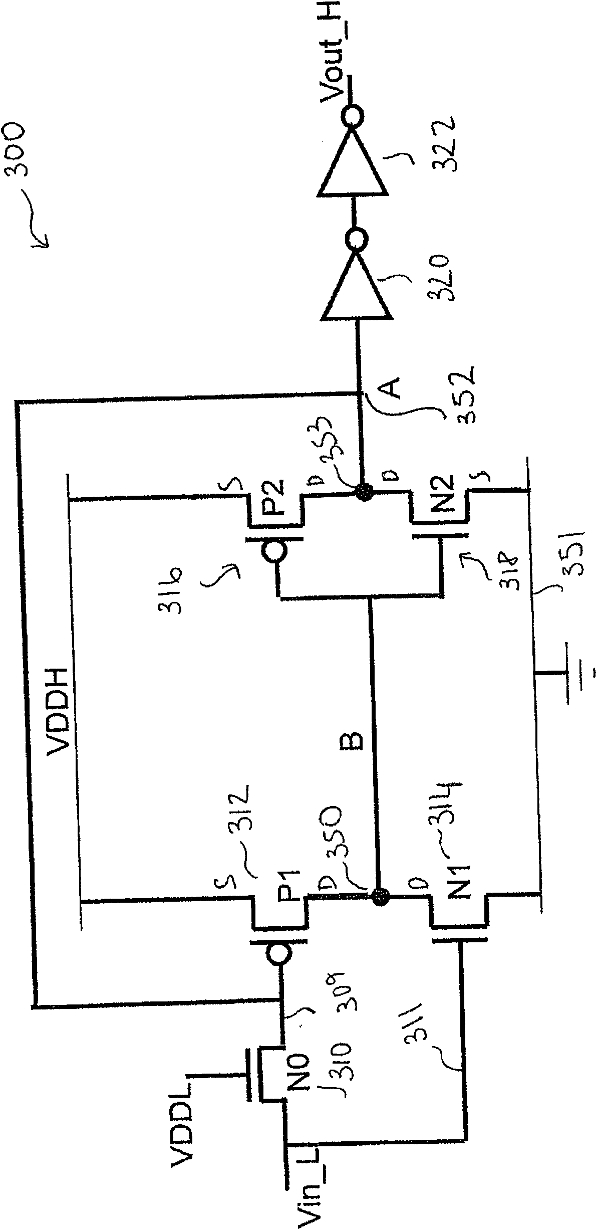
[0051] image 3 A design of a single well voltage level shifter suitable for a standard cell according to a first embodiment of the present invention is schematically illustrated. The circuit includes an NMOS pass transistor 310 and four transistors 312 , 314 , 316 and 318 connected between a high voltage domain VDDH (source voltage) and a ground voltage rail 351 . These four transistors include a first PMOS transistor 312 whose gate is connected to the output terminal of pass transistor 310 and whose source is connected to the high voltage domain VDDH. The drain of PMOS transistor 312 is connected to the drain of NMOS transistor 314 , and the source of NMOS transistor 314 is in turn connected to ground rail 351 .

[0052] The transistor pair including PMOS transistor 316 and NMOS transistor 318 collectively form an inverter circuit. The source of PMOS transistor 316 is connected to the high voltage domain VDDH, while the source of NMOS transistor 318 is connected to ground ...


PUM


Abstract

A voltage level shifter is provided for receiving an input signal from an input voltage domain and converting said signal to a shifted signal in a shifted voltage domain. The voltage level shifter has an input, switching circuitry, a pass transistor and an output. The switching circuitry is configured to isolate an output of said pass transistor from said supply voltage rail when said input voltage domain corresponds to a logical zero.

Description

technical field [0001] The technical field of the invention relates to voltage level shifters for shifting voltage levels between two different voltage domains. Background technique [0002] It is known to provide a voltage level shifter to convert a signal from one voltage domain to a signal suitable for another voltage domain. It allows circuits operating at different voltage levels to interface with each other. [0003] In application-specific integrated circuit (ASIC) design, the circuit design is usually performed by implementing a standard cell (Standard Cell). In this way, ASIC manufacturers can create functional blocks with known electrical characteristics such as propagation delay, capacitance, and inductance that can be expressed in third-party circuit design tools. Standard cell design utilizes these functional blocks to achieve high equivalent gate density (gate density) and good electrical performance. The constraints on circuit components (eg electrical char...

Claims


Application Information

Patent Timeline
Patent Type & Authority Applications(China)
IPC IPC(8): H03K19/185
CPCH03K19/018521H03K3/356113
Inventor A·W·阿拉姆
Owner ARM LTD
Why Eureka
Try Eureka