Printed circuit board(PCB) with thicker inner-layer baseplates

A PCB board and inner layer technology, applied in the direction of circuit substrate materials, printed circuit components, etc., can solve the problems of easy cardboard, easy warping of board corners, etc., to improve quality, reduce PCB board scrapping, and reduce enterprise costs Effect

Inactive Publication Date: 2011-01-12
昆山元茂电子科技有限公司
View PDF3 Cites 8 Cited by
  • Summary
  • Abstract
  • Description
  • Claims
  • Application Information

AI Technical Summary

Problems solved by technology

[0004] In order to solve the problem in the prior art that when the inner layer substrate is arranged for the DES line and the lamination line, the board corners are easy to warp, and the inner layer substrate is easily jammed when directly placed, the present invention provides a simple structure, the inner layer The thickness of the substrate is relatively thick, and the PCB board is not easy to be stuck when placed

Method used


Image

  • Printed circuit board(PCB) with thicker inner-layer baseplates
  • Printed circuit board(PCB) with thicker inner-layer baseplates

Examples


Embodiment Construction

[0014] The present invention will be further described below in conjunction with the accompanying drawings.

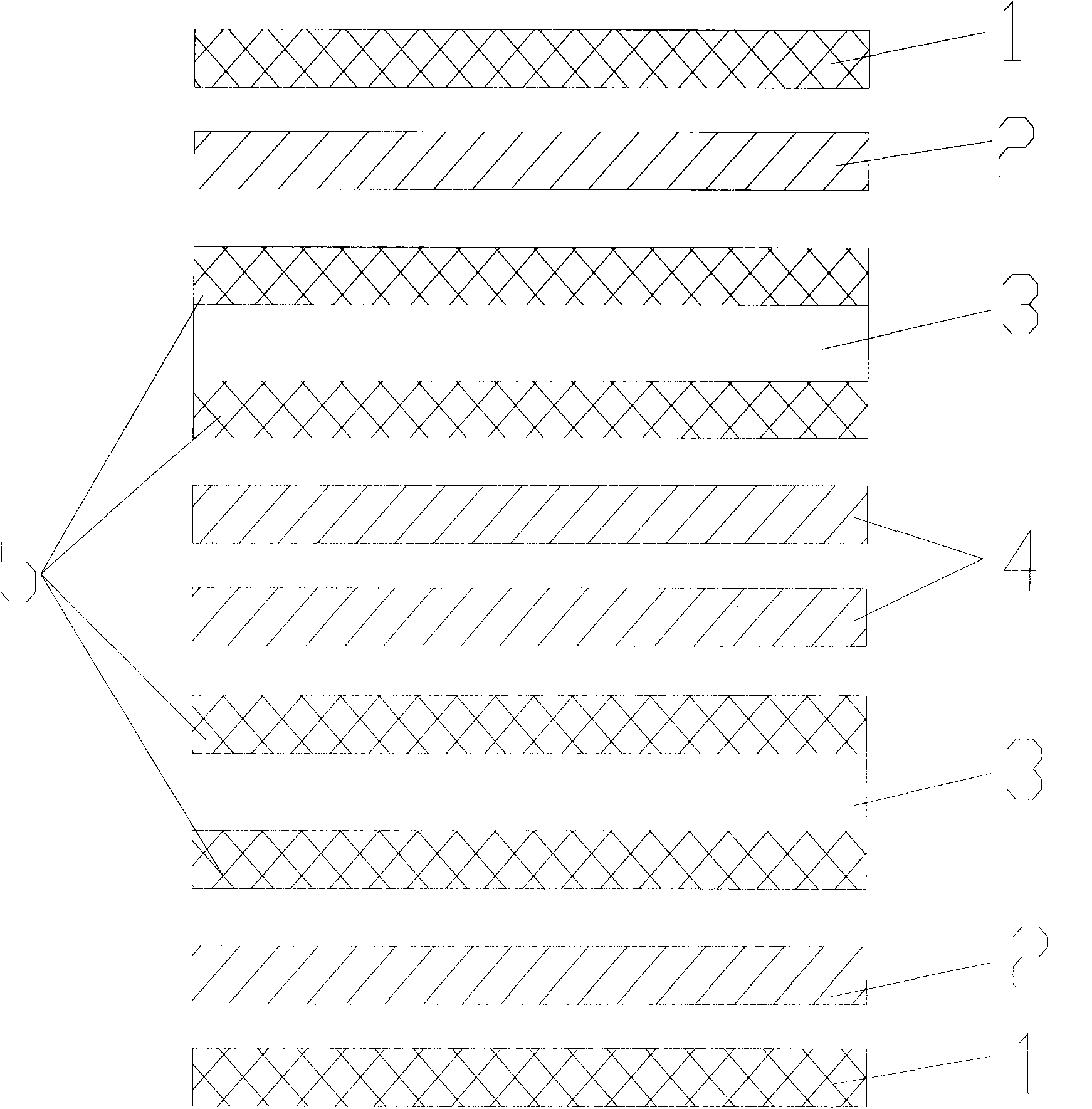
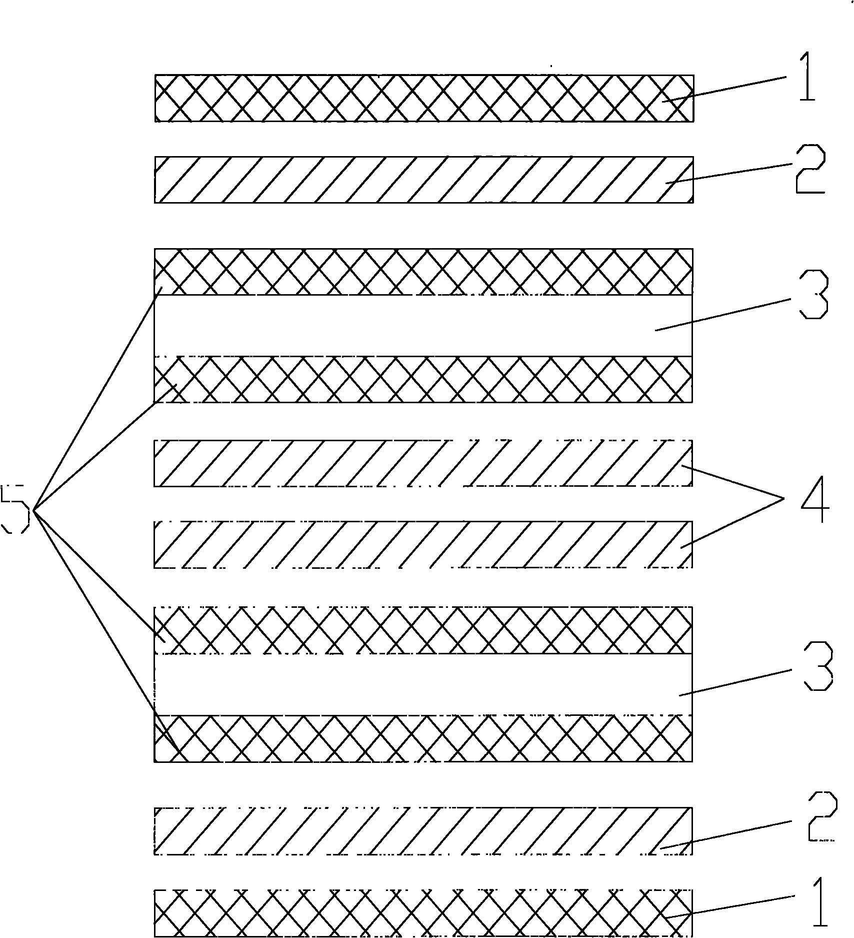
[0015] like figure 1 As shown, a PCB board provided with a thicker inner substrate includes two outer layers of copper foil 1, two outer layers of PP2, two inner layers of substrate 3 and inner layer PP4, the two outer layers of copper foil 1 are located on the outermost side, and the two outer layers of copper foil 1 are located on the outermost side. The thickness of the outer copper foil 1 is 1.780mil. Two outer layers of PP2 are arranged on the inside of the outermost two outer layers of copper foil 1. The material used for the two outer layers of PP2 is PP1080. The two outer layers of PP2 include an upper layer of PP and a lower layer of PP. The thickness is 2.977mil. Two inner layer substrates 3 are arranged inside the two outer layers PP2, the thickness of each inner layer substrate 3 is 4mil, and inner layer copper foils 5 are arranged on both sides of each i...


PUM


Abstract

The invention discloses a Printed circuit board(PCB) with thicker inner-layer baseplates, relating to the technical field of printed circuit board. The Printed circuit board(PCB) comprises two outer-layer copper foils at the outermost side and two outer-layer PPs arranged at the inner side of the two outer-layer copper foils, and the outer-layer pps are made of PP1080. The Printed circuit board(PCB) is characterized by further comprising two inner-layer baseplates and inner-layer PPs, the inner sides of the two outer-layer PPs are provided with two inner-layer baseplates, and the inner-layer baseplates have the thickness of 4 mil. The two sides of each inner-layer baseplate are provided with inner-layer foils, the inner sides of the two inner-layer baseplates are provided with inner-layer PPs, the inner-layer PPs comprise two layers of PP, and the two layers of PP are made of PP7630. The invention solves the problem that in the prior art, when DES wires are arranged and multibond wires are pressed, the corners of the inner-layer baseplates can be warped easily, and the inner-layer baseplates can be blocked easily when being arranged directly. The invention provides the PCB which has simple structure, and the inner-layer baseplates of the PCB are thicker and can not be blocked easily when being arranged.

Description

technical field [0001] The invention relates to the technical field of printed circuit boards, in particular to a PCB board provided with a thicker inner substrate. Background technique [0002] PCB (Printed Circuit Board), the Chinese name is printed circuit board, also known as printed circuit board, printed circuit board, is an important electronic component, a support for electronic components, and a provider of electrical connections for electronic components. Because it is made using electronic printing, it is called a "printed" circuit board. PCB production process: sending material→inner layer→internal inspection→pressing→drilling→plating one copper→outer layer (exposure, development)→plating two copper→tinning→SES (removing film, etching, stripping tin)→proof Welding → processing → text → forming → final inspection → final inspection (FQC) → OQC → packaging → storage. The inner layer and lamination process are as follows: inner layer process: pre-treatment → film ...

Claims


Application Information

Patent Timeline
Patent Type & Authority Applications(China)
IPC IPC(8): H05K1/03
Inventor 田锋罗育光
Owner 昆山元茂电子科技有限公司
Why Eureka
Try Eureka