Method for coating photoresist and method for forming photolithography pattern

A coating method and photoresist technology, applied in the direction of photo-engraving process coating equipment, etc., can solve the problems affecting the line width of the exposure process, etching or ion implantation, photolithography pattern defects, etc., to eliminate defects and improve good quality. The effect of low gas rate and gas cost

Inactive Publication Date: 2009-01-28
SEMICON MFG INT (SHANGHAI) CORP
View PDF1 Cites 17 Cited by
  • Summary
  • Abstract
  • Description
  • Claims
  • Application Information

AI Technical Summary

Problems solved by technology

[0011] In the step of forming a photoresist layer by the spin-coating method, it is necessary to spray cleaning liquid to the backside edge of the semiconductor wafer to clean (Backrinse) the backside of the semiconductor wafer to remove the pollution caused by the photoresist flowing to the backside along the edge of the semiconductor wafer , the pollution will pollute the loading stage of the exposure machine through the semiconductor wafer, which will affect the line width of the exposure process
[0012] However, when the back of the semiconductor wafer is cleaned by cleaning liquid, since the semiconductor wafer is in a rotating state, the solvent sprayed on the back of the semiconductor wafer will be thrown to the side wall of the spin coating equipment, and will be splashed (Spatter) to the photoresist. The surface of the layer, causing defects (Defect), which further makes the formed photolithographic pattern have defects, and causes defects in etching or ion implantation

Method used


Image

  • Method for coating photoresist and method for forming photolithography pattern
  • Method for coating photoresist and method for forming photolithography pattern
  • Method for coating photoresist and method for forming photolithography pattern

Examples


Embodiment Construction

[0056] The specific embodiments of the present invention will be described in detail below in conjunction with the accompanying drawings.

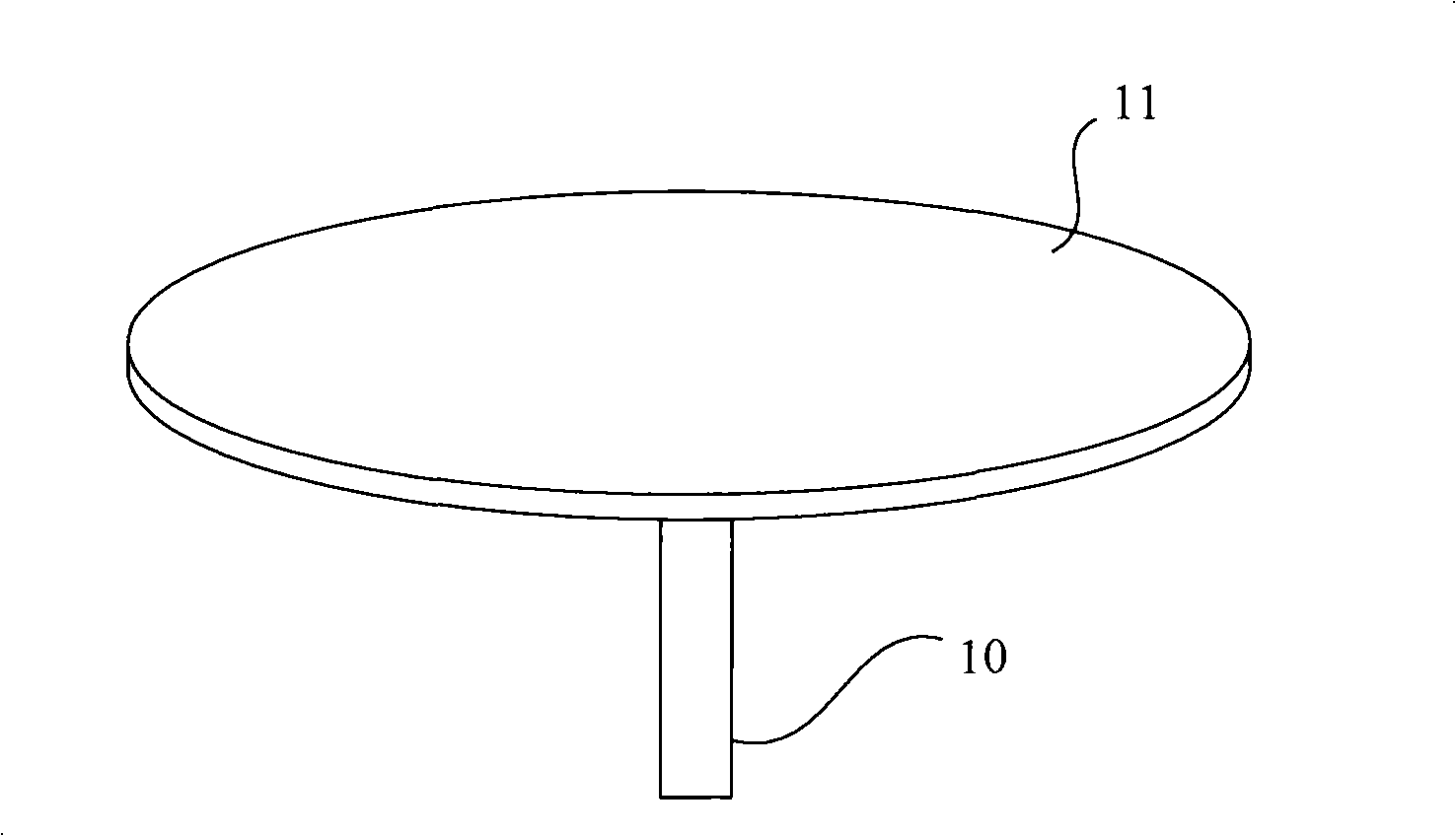
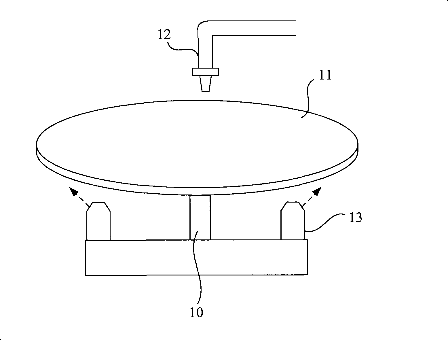
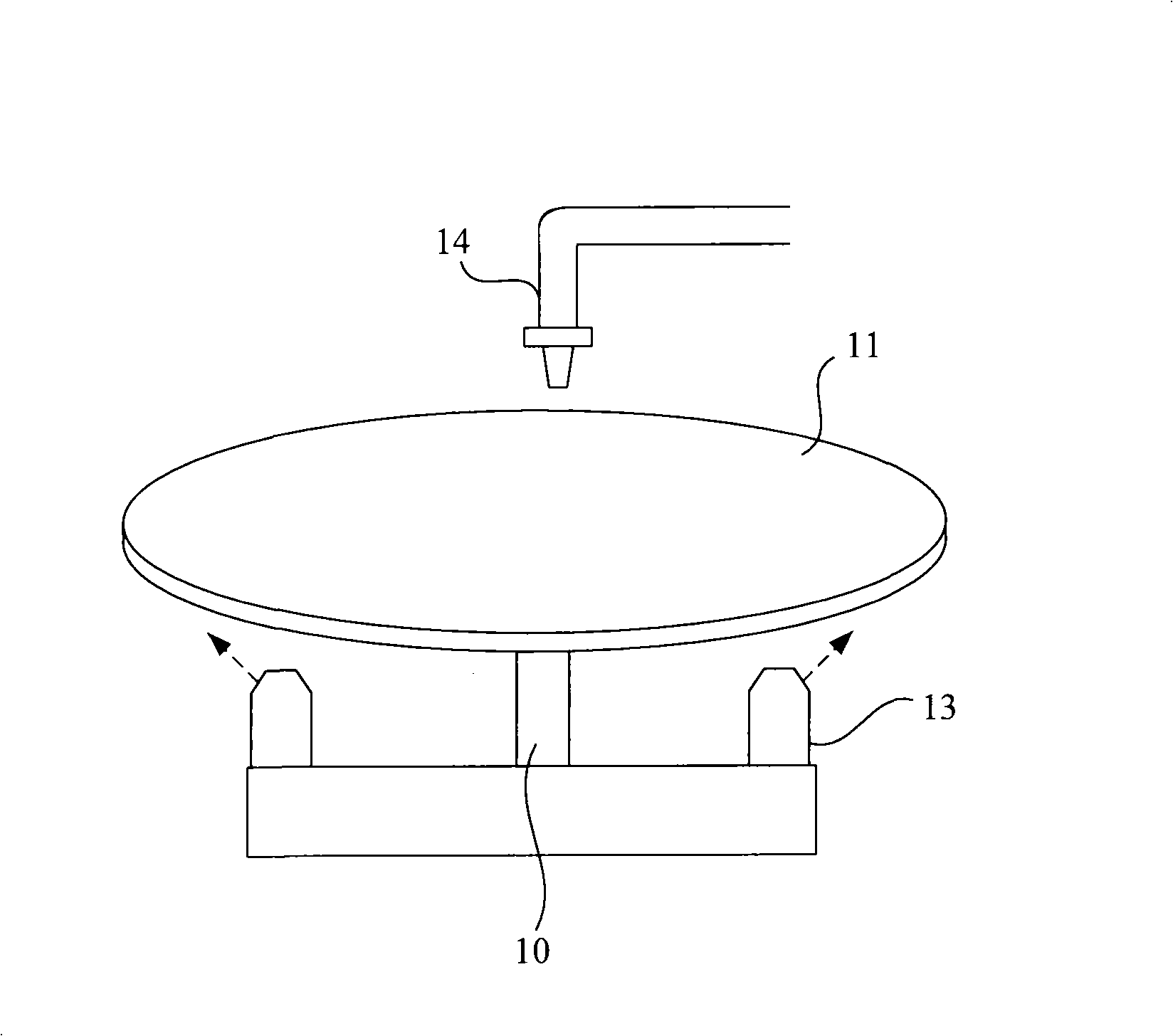
[0057] In the photoresist coating process, in order to prevent the photoresist from flowing to the back side along the edge of the semiconductor wafer and causing pollution, it is necessary to spray a cleaning solution on the back of the semiconductor wafer for cleaning; however, the cleaning process of the cleaning solution is accompanied by the cleaning of the semiconductor wafer. Rotate, so that the cleaning solution sprayed on the back of the semiconductor wafer is thrown to the side wall of the spin coating device, and is splashed back to the surface of the photoresist layer, causing defects. The invention provides a coating method for photoresist, which The method can avoid the occurrence of said defects.

[0058] The step of the coating method of photoresist of the present invention is as follows: first, provide the semiconductor wa...


PUM


Abstract

The invention discloses a photoresist coating method, which comprises the following steps of providing a semiconductor chip; rotating the semiconductor chip and spraying the photoresist on the area of the center or close to the center of the surface of the semiconductor chip, wherein, in the process of rotating the semiconductor chip, spraying gas to the nearly marginal area of the back of the semiconductor chip to prevent the photoresist from being coated on the back along the margin of the semiconductor chip. The invention also provides a formation method of lithography patterns, which can reduce or eliminate the defects caused by back washing.

Description

technical field [0001] The invention relates to the technical field of semiconductor manufacturing, in particular to a method for coating photoresist and a method for forming photolithography patterns. Background technique [0002] In the semiconductor manufacturing process, integrated circuits with various functions are formed on the semiconductor wafer through a series of processes such as photolithography, etching, doping, film deposition, planarization, and cleaning. The photolithographic process of the area plays a very important role. [0003] In the photolithography process, a photoresist layer is first formed on a semiconductor wafer; then the photoresist layer is baked and placed in an exposure device, and the photoresist layer is exposed through an exposure process, The pattern on the mask plate is transferred to the photoresist layer; then the exposed photoresist layer is post-exposure baked (Post Exposure Bake, PEB), and developed by a developing process to form...

Claims


Application Information

Patent Timeline
Patent Type & Authority Applications(China)
IPC IPC(8): G03F7/16
Inventor 郝静安尹朝丽
Owner SEMICON MFG INT (SHANGHAI) CORP
Why Eureka
Try Eureka