
Illumination system for a microlithographic projection exposure apparatus

A lighting system and microlithography technology, applied in the field of lighting systems, can solve problems such as adverse effects

Active Publication Date: 2011-01-12
CARL ZEISS SMT GMBH
View PDF2 Cites 1 Cited by
  • Summary
  • Abstract
  • Description
  • Claims
  • Application Information

AI Technical Summary

Problems solved by technology

This has a particularly detrimental effect in the case of driving larger MMAs with more than 1000 mirrors, since the driver has to be arranged as close as possible to the MMA with rather small clearances

Method used


Image

  • Illumination system for a microlithographic projection exposure apparatus
  • Illumination system for a microlithographic projection exposure apparatus
  • Illumination system for a microlithographic projection exposure apparatus

Examples


Embodiment Construction

[0052] Lighting system

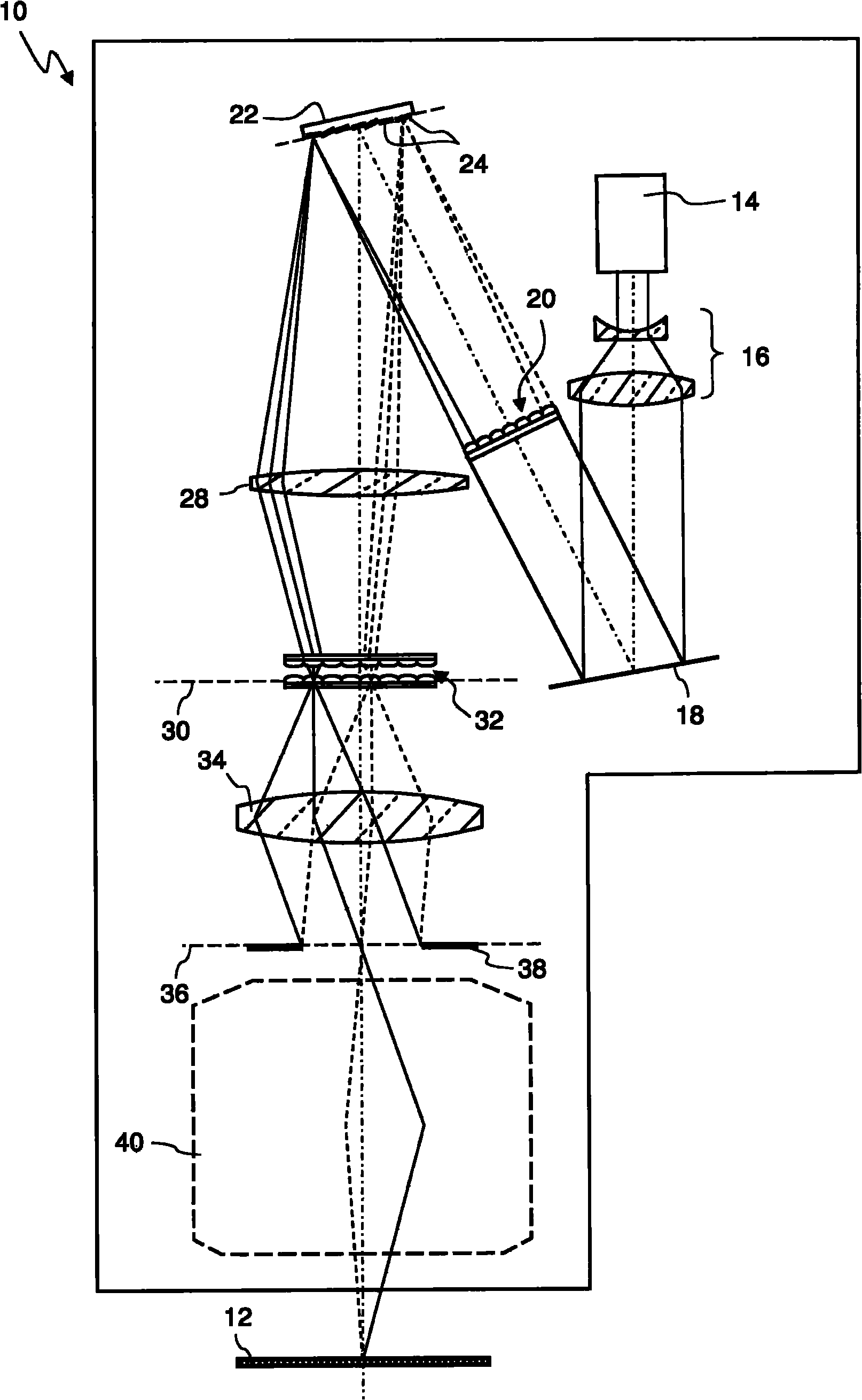
[0053] figure 1 A very simplified meridional cross-section of an illumination system 10 of a projection exposure apparatus for microlithography is shown. The illumination system 10 is used to illuminate with projected light a mask 12 carrying a lithographic structure to be imaged. A projection objective (not shown) then projects the illuminated structures onto the photoresist-coated wafer, typically in reduced size.

[0054] An important factor that decisively influences the imaging properties of a projection exposure system for microlithography is the angular distribution of the projection light. This is understood to mean the distribution of the total intensity of the light impinging on a mask spot which strikes it at different angles of incidence. In particular, it is desirable that the angular distribution of the projected light be adapted to the type of structure to be illuminated in order to obtain the best possible imaging.

[0055] For this...


PUM


Abstract

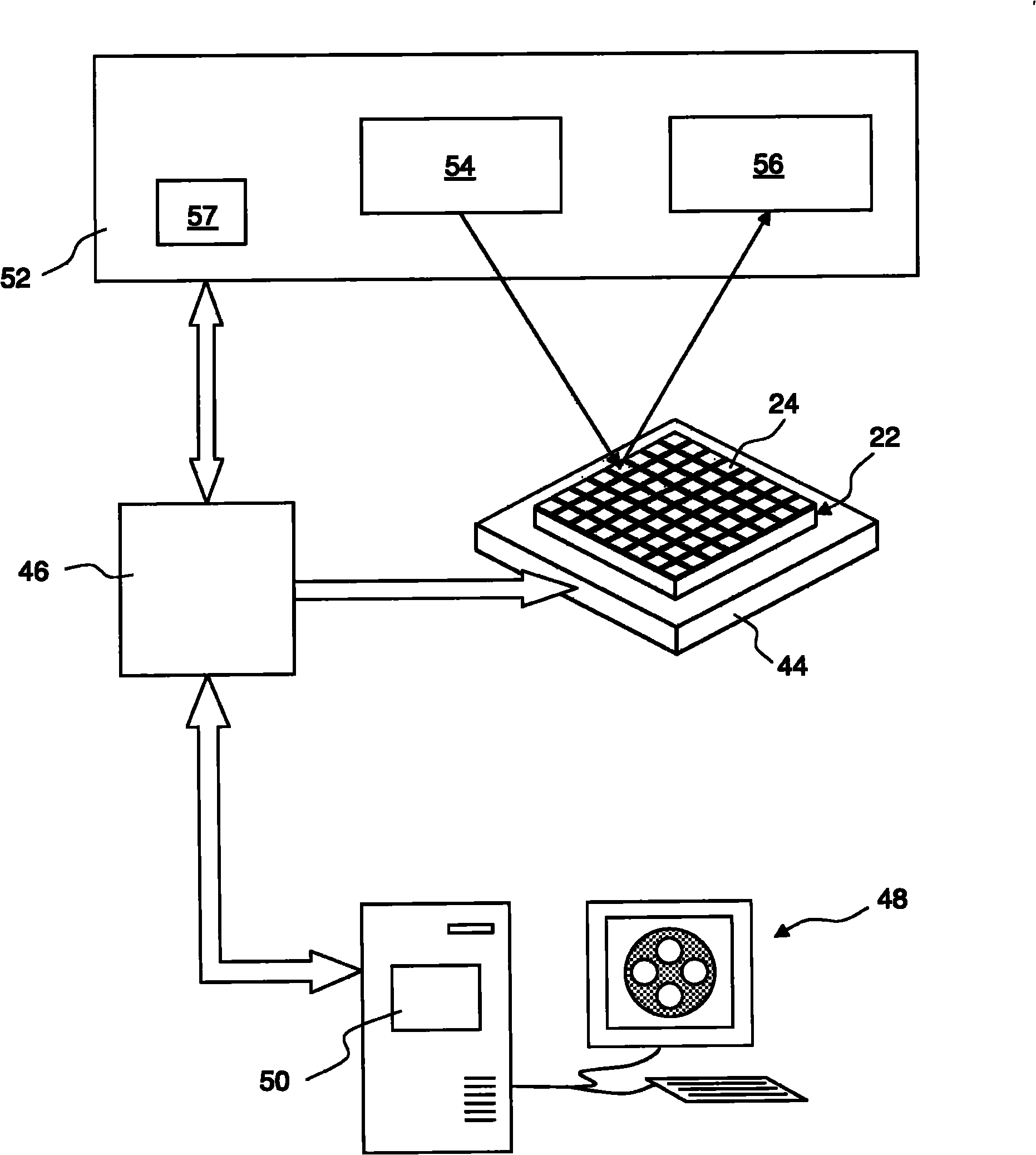
An illumination system for a microlithographic projection exposure apparatus exhibits a mirror which is arranged in a multi-mirror array and is capable of being tilted via at least one actuator. Furthermore, the illumination system exhibits drive electronics for the mirror, which exhibit a coarse digital-to-analogue converter (68) with a first resolution, a fine digital-to-analogue converter (70)with a second resolution, the second resolution being higher than the first resolution, and an adder (72) with which output quantities that are output by the two digital-to-analogue converters (68, 70) are capable of being added to yield an overall quantity. The overall quantity is capable of being applied at least indirectly to the at least one actuator of the mirror.

Description

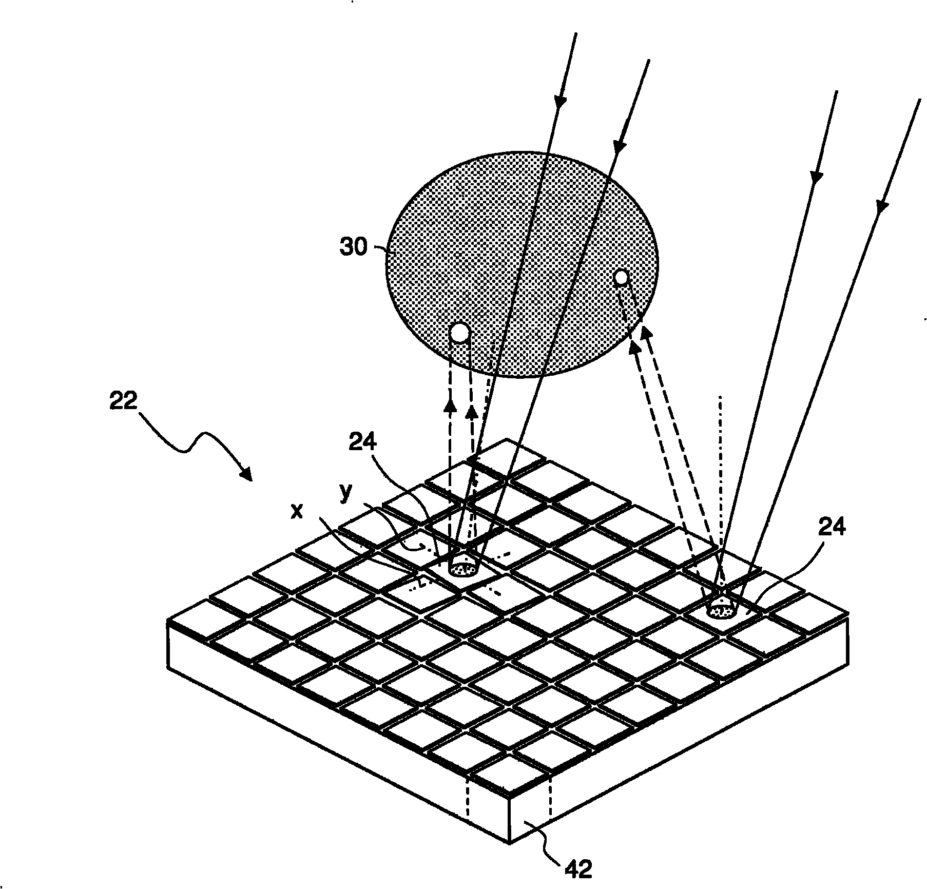
technical field [0001] The invention relates to an illumination system for a projection exposure apparatus for microlithography, having a mirror arranged as a multi-mirror array and capable of tilting via at least one driver, and drive electronics for the mirror, as well as to the drive of the mirror method. Background technique [0002] Integrated circuits and other microstructural components are traditionally fabricated by applying several structural layers to a suitable substrate, which may be, for example, a silicon wafer. For the purpose of structuring said layers, the substrate is first coated with a photoresist which is sensitive to light belonging to a specific wavelength region, for example light in the deep ultraviolet spectral region (DUV). Next, the wafers that have been coated in this way are exposed in a microlithographic projection exposure apparatus. In this process, a pattern of structures arranged on a mask is imaged onto the photoresist by means of a pro...

Claims


Application Information

Patent Timeline
Patent Type & Authority Applications(China)
IPC IPC(8): G03F7/20
CPCG03F7/70116
Inventor 简·霍恩克里斯琴·肯普特沃尔夫冈·法洛特-伯格哈特
Owner CARL ZEISS SMT GMBH
Learn More