Supercharge Your Innovation With Domain-Expert AI Agents!

Suppressing fractures in diced integrated circuits

A technology for integrated circuits and dielectric layers, applied in the field of splitting IC dies, which can solve problems such as reduced adhesive strength, early failure of yield loss, and low dielectric rupture toughness.

Inactive Publication Date: 2011-01-19
LSI CORP
View PDF0 Cites 7 Cited by
  • Summary
  • Abstract
  • Description
  • Claims
  • Application Information

AI Technical Summary

Problems solved by technology

This vulnerability arises from the lower fracture toughness of low-k and ultra-low-k dielectrics relative to silicon dioxide and fluorine-doped silicon dioxide, as well as the lack of adhesion strength between different layers of the dielectric and between the dielectric and copper. reduce
These characteristics can lead to significant yield loss and early failure of ICs utilizing low-k dielectrics

Method used


Image

  • Suppressing fractures in diced integrated circuits
  • Suppressing fractures in diced integrated circuits
  • Suppressing fractures in diced integrated circuits

Examples


Embodiment Construction

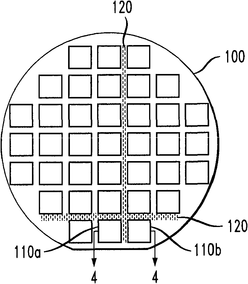
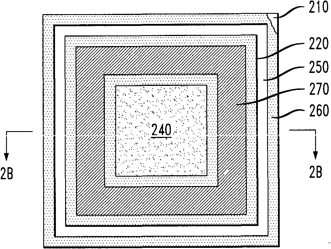
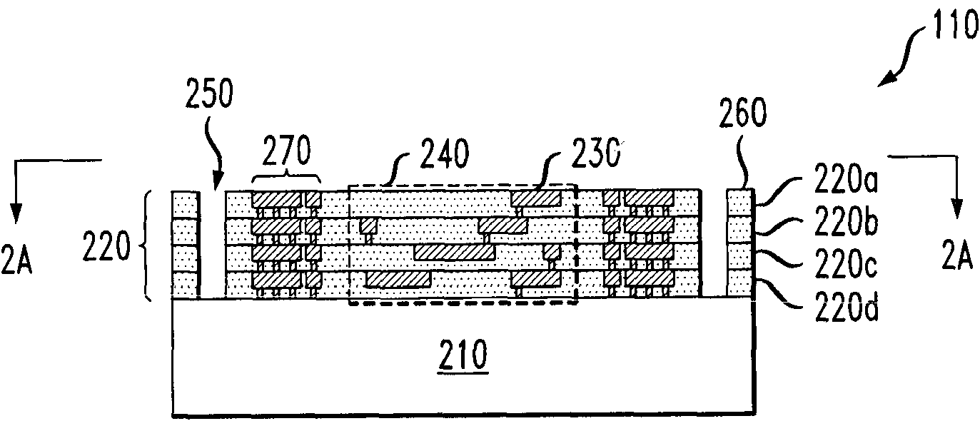
[0016] In some cases, the sealing ring structure cannot prevent the propagation of edge defects. For example, ICs are typically separated in a process called disassembly. One singulation method uses a wafer sawing process (e.g., a rotating grinding wheel) to remove a portion of the substrate (e.g., wafer) and overlying layers in the dicing street between separated integrated circuit dies . The stresses created by the saw blade on the substrate and the dielectric and metal layers formed on the substrate sometimes lead to defects propagating through the seal ring. This defect may result in immediate yield loss, or may result in premature failure of the electronic device.

[0017] Embodiments herein reflect the recognition that propagation of defects initiated during singulation can be prevented by forming a dielectric-free zone between the dicing line and the seal ring. When a defect forms, it can propagate into the dielectric-free region. However, propagation of defects is ...


PUM


Abstract

The invention relates to suppressing fractures in diced integrated circuits. A semiconductor device has a singulated die having a substrate and a die edge. An interconnect dielectric layer is located on the substrate, and integrated circuit has interconnections located within the interconnect dielectric layer. A trench is located in the interconnect dielectric layer and between a seal ring and a remnant of the interconnect dielectric layer. The seal ring is located within the interconnect dielectric layer and between the trench and the integrated circuit, with the remnant of the interconnect dielectric layer being located between the trench and the edge of the die.

Description

technical field [0001] The present invention relates generally to integrated circuits (ICs) and, more particularly, to singulating IC dies. Background technique [0002] Low-k and ultra-low-k dielectrics and copper metallization are used to improve performance in leading-edge silicon technologies. Although they offer lower dielectric constant and resistivity, respectively, copper interconnects and stacks of these dielectrics can be mechanically fragile. This vulnerability arises from the lower fracture toughness of low-k and ultra-low-k dielectrics relative to silicon dioxide and fluorine-doped silicon dioxide, as well as the lack of adhesion strength between different layers of the dielectric and between the dielectric and copper. reduce. These characteristics can lead to significant yield loss and early failure of ICs utilizing low-k dielectrics. [0003] To ameliorate these problems, it is common practice to add reinforcement structures called seal rings around the edg...

Claims


Application Information

Patent Timeline
Patent Type & Authority Applications(China)
IPC IPC(8): H01L23/58H01L21/60
CPCH01L23/5329H01L23/3128H01L23/562H01L2924/19041H01L23/585H01L2924/0002H01L2924/00
Inventor M·A·巴克曼J·W·奥森巴赫
Owner LSI CORP
Features
  • R&D
  • Intellectual Property
  • Life Sciences
  • Materials
  • Tech Scout
  • Unparalleled Data Quality
  • Higher Quality Content
  • 60% Fewer Hallucinations
Learn More