Switch direct-current boosted circuit, boosted device and LED illuminating system

A technology of a DC booster circuit and a booster device, applied in the power supply field, can solve the problems of low circuit work efficiency, small voltage rise, large switching loss, etc., and achieve the effects of improving work efficiency, improving rise, and high constant current accuracy.

Inactive Publication Date: 2011-01-19
SHENZHEN SED IND +1
View PDF3 Cites 9 Cited by
  • Summary
  • Abstract
  • Description
  • Claims
  • Application Information

AI Technical Summary

Problems solved by technology

[0004] The purpose of the present invention is to provide a switching DC boost circuit, which aims to solve the problems of the existing switching DC boost circuit, such as large switching loss, low circuit working efficiency, and small voltage increase.

Method used


Image

  • Switch direct-current boosted circuit, boosted device and LED illuminating system
  • Switch direct-current boosted circuit, boosted device and LED illuminating system
  • Switch direct-current boosted circuit, boosted device and LED illuminating system

Examples


Embodiment 1

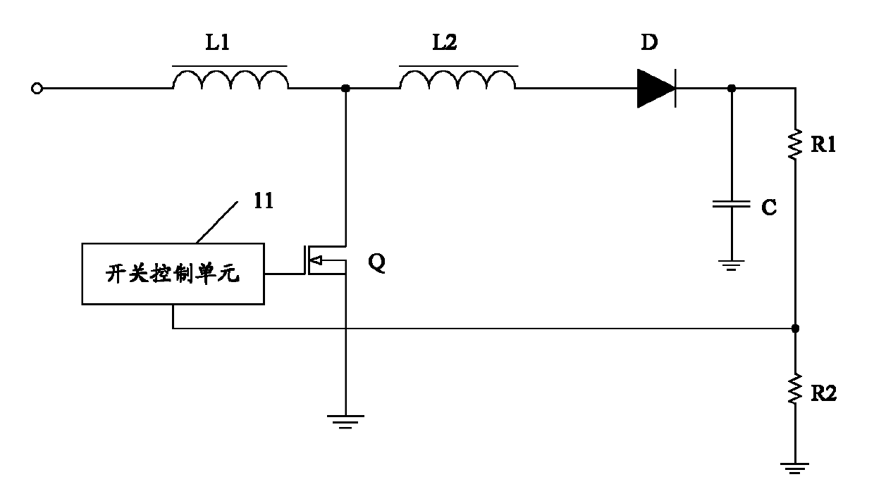
[0028] figure 2 The structure of a switching DC boost circuit provided by an embodiment of the present invention is shown, and only the parts related to the embodiment of the present invention are shown for convenience of description.

[0029] The circuit includes an inductor L1, a diode D, a MOS transistor Q, a capacitor C, a switch control unit 11, a resistor R1, a resistor R2 and an inductor L2.

[0030] Among them, the inductance L1 and the DC voltage input terminal V in connect.

[0031] The inductor L1, the inductor L2, the diode D and the capacitor C are connected in series, and the other end of the capacitor C is grounded.

[0032] The branch formed by the resistor R1 and the resistor R2 is connected in parallel with the capacitor C, and the other end of the resistor R2 is grounded.

[0033] The drain of the MOS transistor Q is connected between the first inductor L1 and the second inductor L2 , the gate is connected to the switch control unit 11 , and the source i...

Embodiment 2

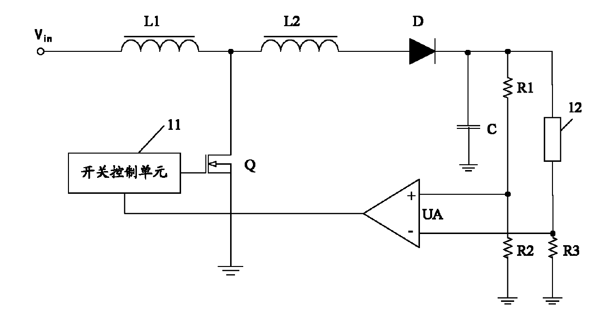
[0038] image 3 The structure of another switching DC boost circuit provided by another embodiment of the present invention is shown, and only the parts related to the embodiment of the present invention are shown for convenience of description.

[0039] The circuit includes an inductor L1, an inductor L2, a diode D, a capacitor C, a resistor R1, a resistor R2, a detection resistor R3, a MOS transistor Q, a switch control unit 11 and a comparator UA.

[0040] Wherein, the positive input terminal of the comparator UA is connected between the resistors R1 and R2 , the negative input terminal of the comparator UA is connected between the load 12 and the detection resistor R3 , and the output terminal of the comparator UA is connected to the switch control unit 11 .

[0041] In actual work, a reference voltage is set. In the embodiment of the present invention, the voltage on the branch formed by resistance R1 and resistance R2 is V 支路 , then the reference voltage V 参考 for V 支路...

Embodiment 3

[0044] The switching direct current boosting circuit provided in the embodiment of the present invention can be widely used in various boosting devices, and these boosting devices can be used in fields such as LED lighting systems. When applied to an LED lighting system, the load 12 is an LED lamp group.

[0045] The embodiment of the present invention solves the problems of large switching loss and small voltage increase in the existing switching DC boosting circuit by adding a new inductor to the existing switching DC boosting circuit. There are beneficial effects such as improving the working efficiency, improving the voltage rise, and realizing high constant current accuracy.


PUM


Abstract

The invention is suitable for the field of power supply, and provides a switch direct-current boosted circuit, a boosted device and an LED illuminating system. The switch direct-current boosted circuit comprises an inductor L1, an inductor L2, a diode D, a capacitor C, a resistor R1, a resistor R2, a MOS tube Q and a switch control unit. Due to the addition of the new inductor in the switch direct-current boosted circuit, the problems of large switch loss, small amplitude of voltage rise and the like in the prior art are solved, so that the switch direct-current boosted circuit improves the work efficiency and the amplitude of output voltage rise.

Description

technical field [0001] The invention belongs to the field of power supplies, and in particular relates to a switch DC boost circuit, a boost device and an LED lighting system. Background technique [0002] The switching DC boost circuit (BOOST circuit) is widely used in LED backlight and other fields. The working principle of the existing switching DC boost circuit is as follows: figure 1 shown. The switch control unit controls the turn-on and cut-off of the MOS transistor Q according to the feedback information on the branch composed of the resistor R1 and the resistor R2, and the diode D reverse cut-off. When the MOS transistor Q is turned on, the current of the inductor L1 continues to increase, and the inductor L1 and the capacitor C store energy; when the MOS transistor Q is turned off, the inductor L1 charges the capacitor C through the diode D to complete energy transfer, thereby increasing the output voltage. The switch control unit continuously controls the turn-o...

Claims


Application Information

Patent Timeline
Patent Type & Authority Applications(China)
IPC IPC(8): H02M3/155H05B37/02
Inventor 张子奇马博
Owner SHENZHEN SED IND
Why Eureka
Try Eureka