

Heteroepitaxial growth method for high-quality monocrystalline thick-film material
A heteroepitaxial and epitaxial growth technology, applied in the direction of single crystal growth, crystal growth, chemical instruments and methods, etc., can solve problems such as complex processing technology
- Summary
- Abstract
- Description
- Claims
- Application Information
AI Technical Summary
Problems solved by technology
Method used
Image

Examples
Embodiment Construction
[0030] The method for heteroepitaxial growth of high-quality single-crystal thick-film materials of the present invention will be further described below in conjunction with the accompanying drawings and specific embodiments.
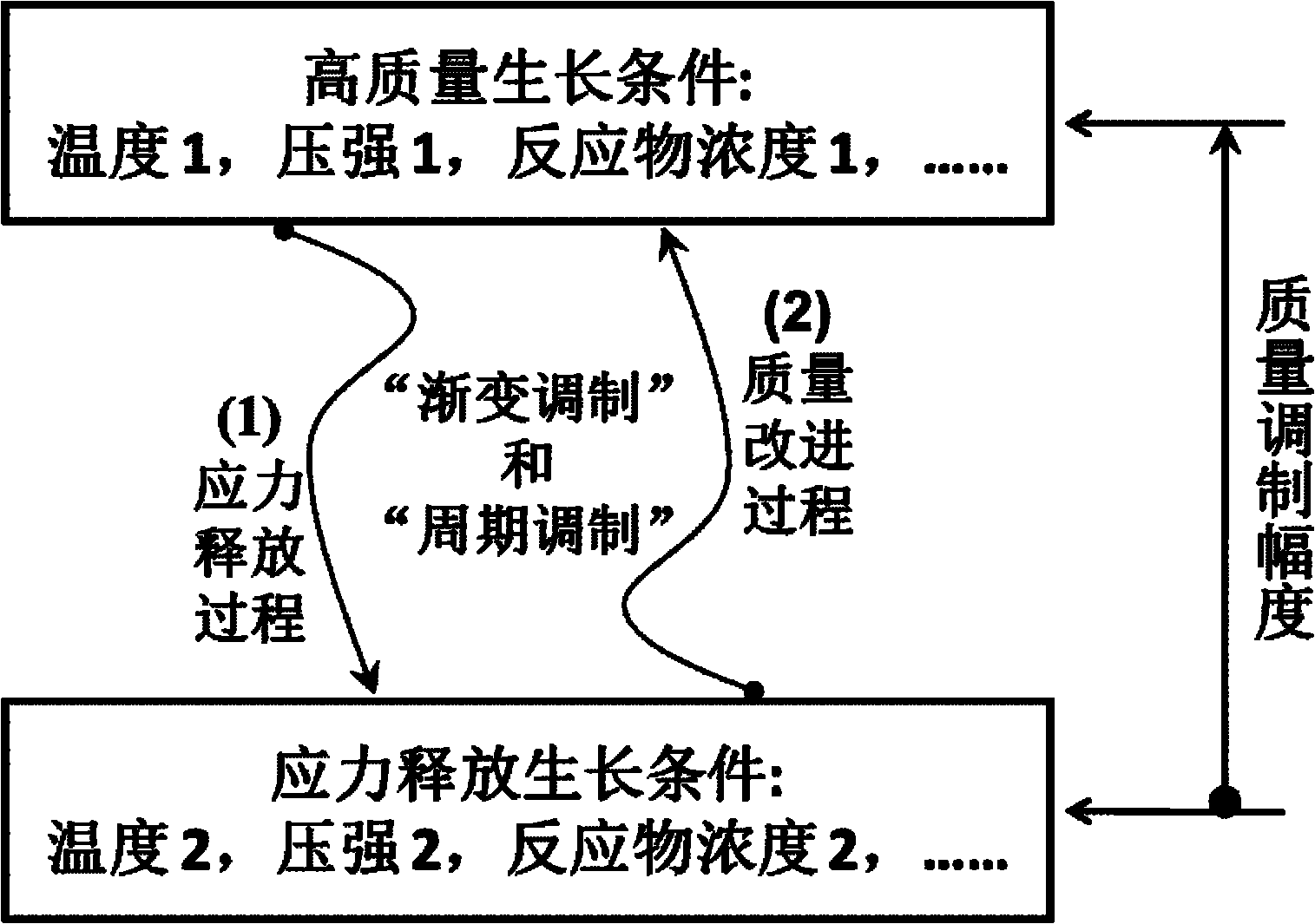
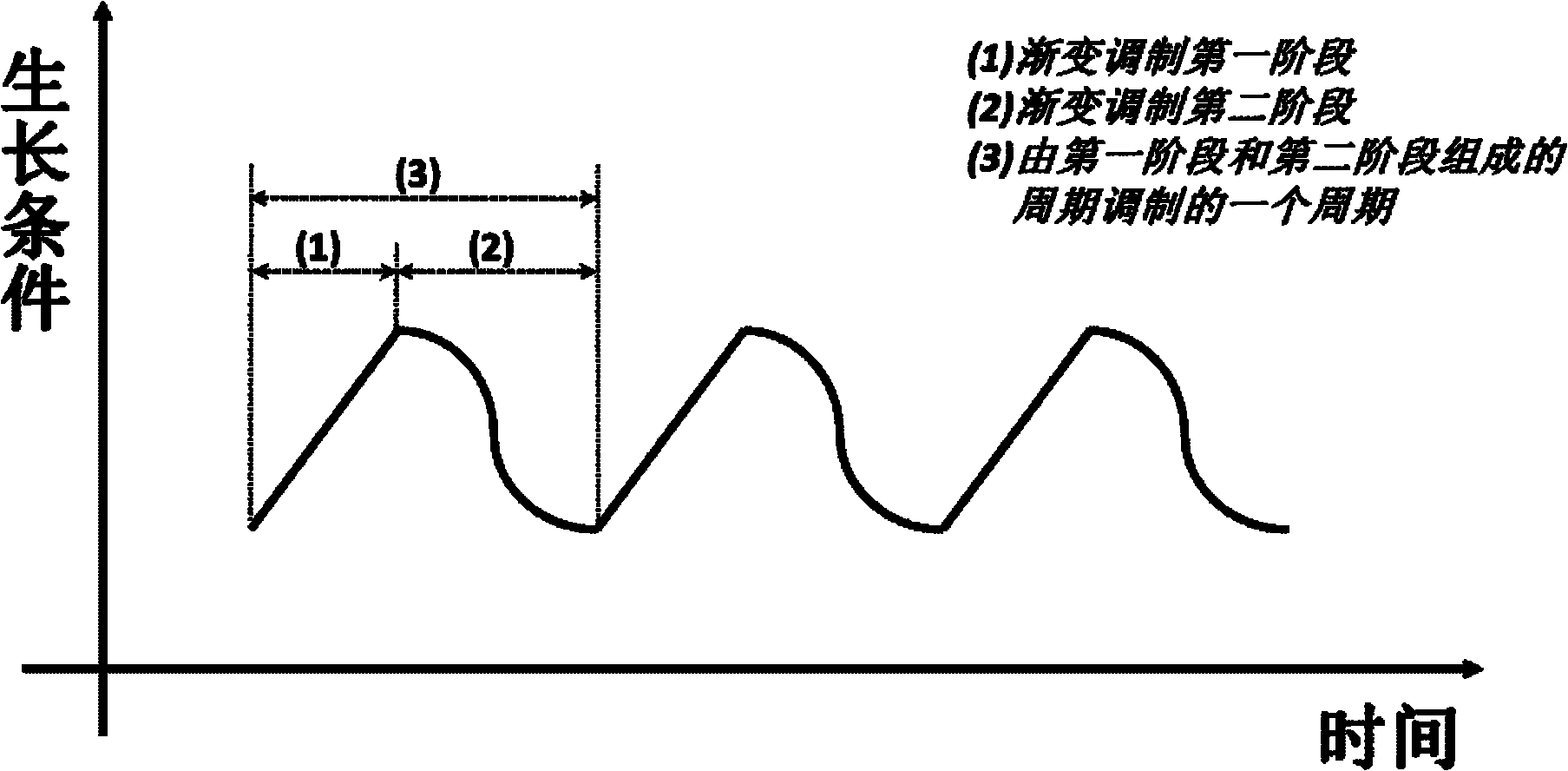
[0031] The design scheme of the present invention is as figure 1 As shown, "gradual modulation" refers to the gradual change of basic process parameters such as temperature, pressure, reaction gas flow rate or reactant concentration and their combinations. The material quality is stable, and at the same time, this gradual change can gradually implement the control of stress release in the epitaxial process. In addition, if the gradual change process follows a certain change function, such as a linear function, then the epitaxy process can be quantified and regularized, which increases the quantitative controllability of the epitaxy process.
[0032] Such as figure 1 As shown, the gradual change process from high-quality growth conditions to stress-rel...
PUM
 Abstract
Description
Claims
Application Information