Method for manufacturing touch panel

A manufacturing method and touch panel technology, applied in the input/output process of data processing, instruments, electrical digital data processing, etc., can solve the problems of high resistance, metal oxidation, and high sensing series resistance, and achieve improved Reliability, reduction of manufacturing cost, effect of reduction of process steps

Active Publication Date: 2011-02-16
AU OPTRONICS CORP
View PDF5 Cites 40 Cited by
  • Summary
  • Abstract
  • Description
  • Claims
  • Application Information

AI Technical Summary

Problems solved by technology

However, the resistance of indium tin oxide (ITO) is too high, which easily leads to the problem of poor sensitivity of the touch panel.
In order to solve the above-mentioned problem of high resistance value, the known technology also proposes to use metal material to replace part of ITO to make the first bridge part or the second bridge part, so as to reduce the problem of high resistance value of the sensing series.
[0004] In order to reduce the process steps of the touch panel and reduce the production cost, manufacturers try to reduce the number of processes of the touch panel. Taking the production of the uppermost insulating layer as an example, if the uppermost insulating layer is not produced, the metal material The first bridging portion or the second bridging portion will be directly exposed to the external environment, which will easily lead to oxidation of the metal, thereby greatly reducing the reliability and service life of the touch panel.
Moreover, if the contact pads connecting the peripheral area of ​​the touch panel to the external circuit are made of metal, the metal contact pads will inevitably be directly exposed to the outside air environment before connecting to the external circuit, which will also easily lead to oxidation of the metal. Then the reliability and service life of the touch panel are greatly reduced

Method used


Image

  • Method for manufacturing touch panel
  • Method for manufacturing touch panel
  • Method for manufacturing touch panel

Examples


Embodiment Construction

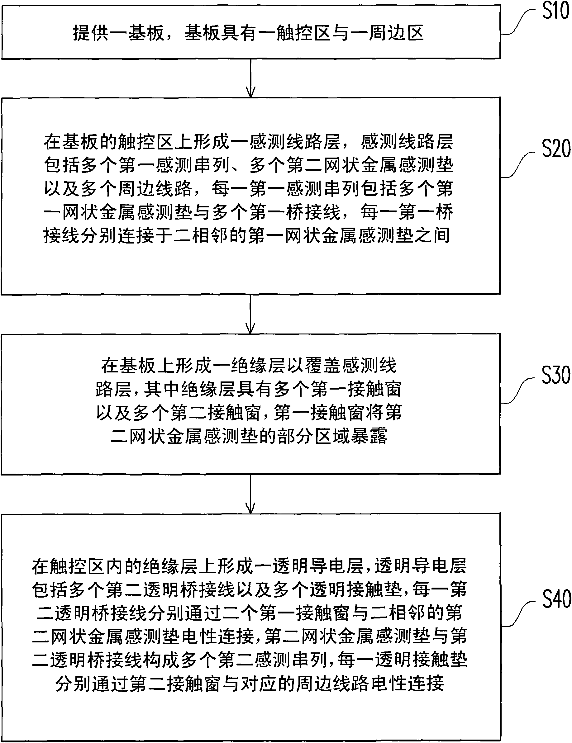
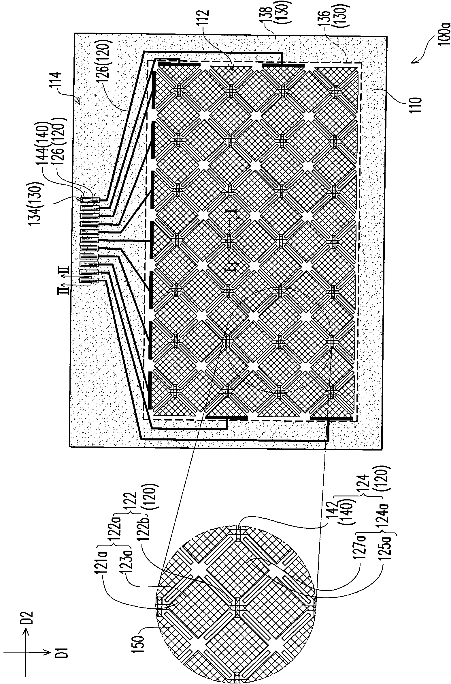
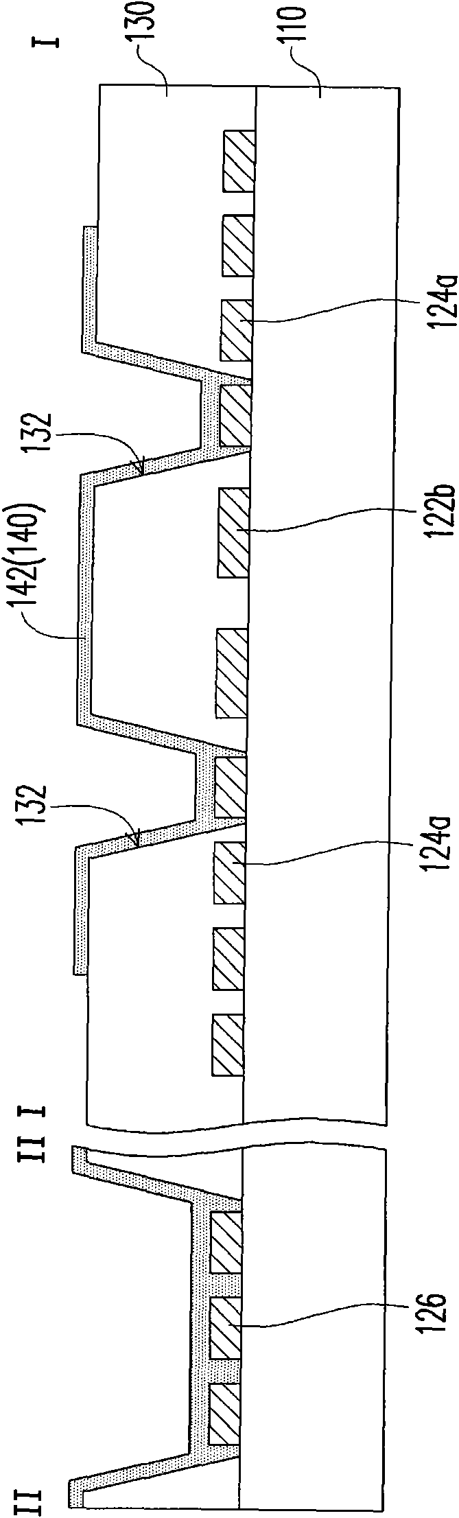
[0045] figure 1 It is a flowchart of a manufacturing method of a touch panel according to an embodiment of the present invention, Figure 2A is a schematic top view of a touch panel according to an embodiment of the present invention, and Figure 2B for along Figure 2A Schematic cross-section of the line I-I. Please also refer to figure 1 and Figure 2A , The manufacturing method of the touch panel of this embodiment includes step S10 to step S40. Firstly, a substrate 110 is provided (step S10 ), wherein the substrate 110 has a touch area 112 and a peripheral area 114 . In this embodiment, the substrate 110 is, for example, a glass substrate, a plastic substrate, a printed circuit board or a display panel.

[0046] Next, please also refer to the figure 1 and Figure 2A , forming a sensing circuit layer 120 on the touch area 112 of the substrate 110 (step S20). In detail, the sensing circuit layer 120 includes a plurality of first sensing series 122, a plurality of se...


PUM


Abstract

The invention relates to a method for manufacturing a touch panel, which comprises the steps of: providing a substrate with a touch area and a periphery area; forming a sensing circuit layer comprising a plurality of first sensing series, a plurality of second cellular metal sensing pads and a plurality of periphery circuits on a touch area of the substrate; forming an insulating layer provided with a plurality of first contact windows and a plurality of second contact windows on the substrate so as to cover the sensing circuit layer; exposing the partial areas of the second cellular metal sensing pads by the first contact windows; and forming a transparent conductive layer comprising a plurality of second transparent bridging lines and a plurality of transparent contact pads on the insulating layer in the touch control area of the substrate, wherein each second transparent bridging line is respectively and electrically connected with two adjacent second cellular metal sensing pads by two first contact windows, and each transparent contact pad is respectively and electrically connected with the corresponding periphery circuits by the second contact windows.

Description

technical field [0001] The present invention relates to a manufacturing method of a touch panel, and in particular to a manufacturing method of a capacitive touch panel. Background technique [0002] Touch panels are roughly classified into resistive touch panels, capacitive touch panels, optical touch panels, acoustic wave touch panels, and electromagnetic touch panels according to their sensing methods. Since the capacitive touch panel has the advantages of fast response time, good reliability and high durability, the capacitive touch panel has been widely used in electronic products. [0003] Generally, the capacitive touch panel includes a plurality of first sensing series extending along a first direction and a plurality of second sensing series extending along a second direction. Wherein, each first sensing series is composed of a plurality of first sensing pads connected in series with a first bridge portion, and each second sensing series is formed of a plurality of...

Claims


Application Information

Patent Timeline
Patent Type & Authority Applications(China)
IPC IPC(8): G06F3/041G06F3/044
Inventor 简钰峰陈政德杨敦钧李锡烈
Owner AU OPTRONICS CORP
Why Eureka
Try Eureka