Method for making solar batteries by adopting ion injection method
A technology of ion implantation and solar cells, applied in circuits, photovoltaic power generation, electrical components, etc., can solve problems such as silicon wafer quality degradation and solar cell performance deterioration, and achieve high conversion efficiency, maximum realization, and power output effects
- Summary
- Abstract
- Description
- Claims
- Application Information
AI Technical Summary
Problems solved by technology
Method used
Image

Examples
Embodiment 1
[0028] Disclosed here is a doping method that does not involve thermal diffusion on n-type crystalline silicon wafers and a design scheme that makes full use of this doping method, which can enable crystalline silicon solar cells to achieve the highest conversion efficiency and power output of maximization.
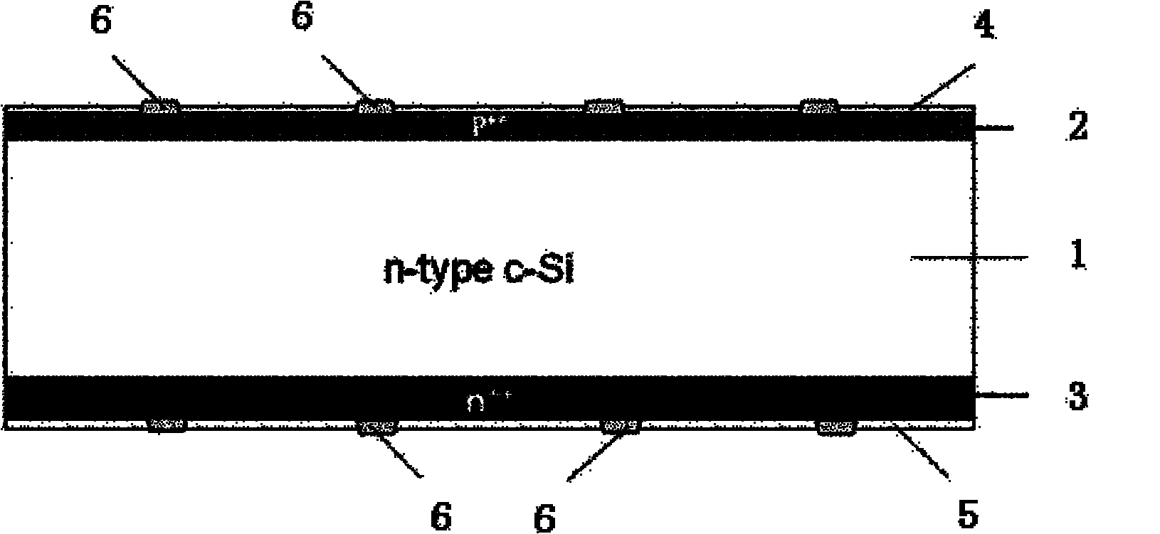
[0029] as attached Figure 1-2 As shown, one embodiment of the present invention is to use n-type crystalline silicon wafers with a resistivity of 0.5 to 15 Ω·cm to make high-efficiency solar cells. The crystalline silicon wafers referred to here may have undergone some other processing steps, such as cleaning and etching. , to remove pollutants and cutting damage layers on the surface of the silicon wafer, or perform anisotropic texturing to form a pyramid structure on the surface of the silicon wafer to increase the light absorption of the silicon wafer.
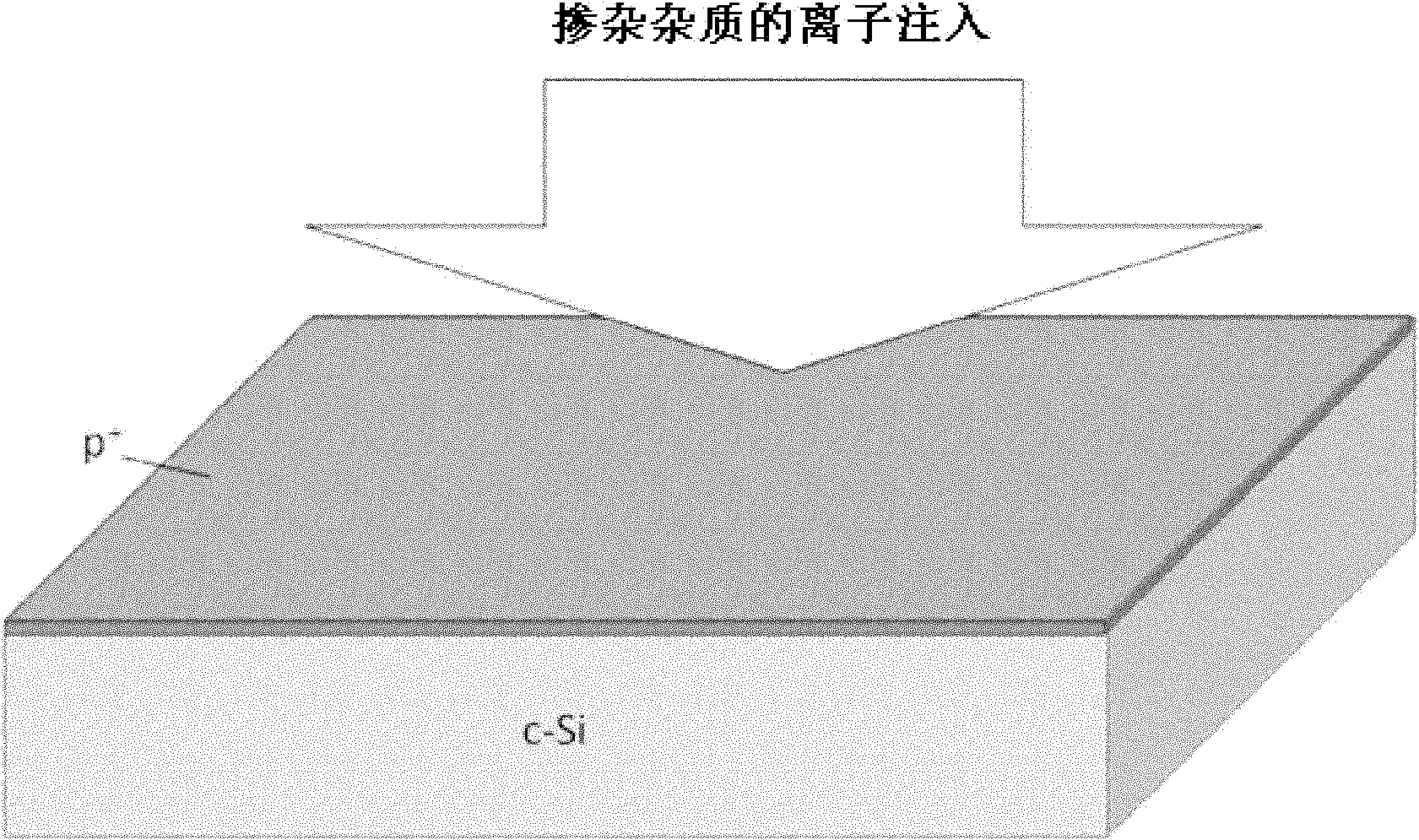
[0030] Active, charged particles can be doped on the first surface of the above-mentioned silicon wafer by ion imp...
Embodiment 2
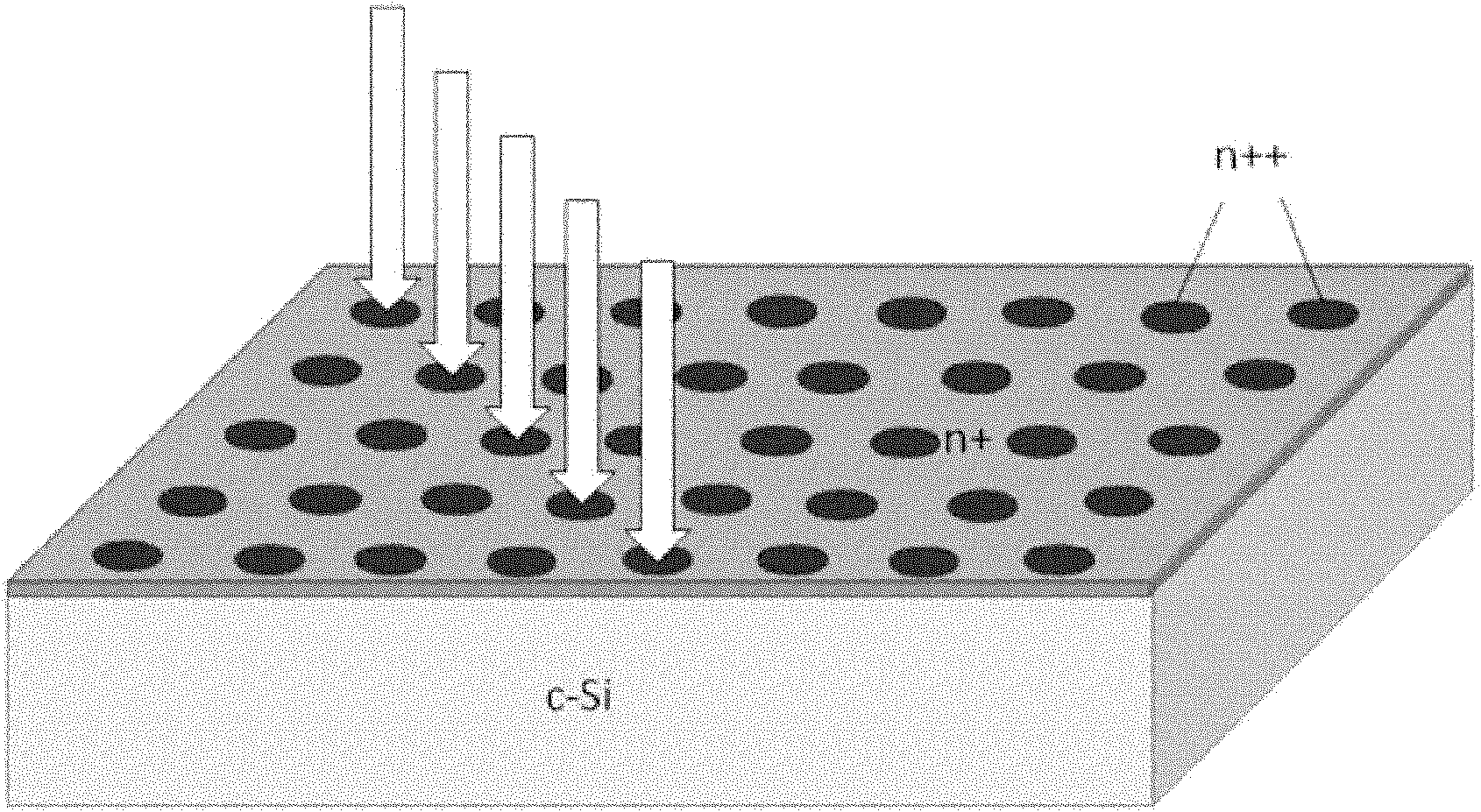
[0036] as attached Figure 3a-3b As shown, on the basis of making a high-efficiency solar cell in Example 1, ion implantation can optimize the design structure of the solar cell, and carry out heavy doping on the local area of the second surface of the silicon wafer, doping with the same conductivity type as the silicon wafer of impurities. As shown in FIG. 3( a ), dotted n++ doped regions are formed on the existing n+ layer. The n+ layer that has existed before can be formed by thermal diffusion, or can be formed by the above-mentioned ion implantation method. In order to form spot doping, a mask needs to be placed in front of the silicon wafer to be doped to ensure precise doping of the target area. The types of impurities forming n-type doping may include but not limited to phosphorus (P), arsenic (As), and antimony (Se). Multiple ion implantation with different ion beam energies can achieve deeper doping profiles.
[0037] In this embodiment, the silicon wafer is a p...
Embodiment 3
[0045] as attached Figures 4a-4c As shown, another preferred way to make high-efficiency solar cells is to use a crystalline silicon wafer with a resistivity of 0.5-15 Ω·cm, and use ion implantation doping to make the heavily doped n++ and p++ regions located on the silicon wafer. On the same surface, n-type and p-type doped ion beams are sequentially implanted using a pair of masks. The p-type dopant can be implanted on one surface of the n-type crystalline silicon wafer using a mask with opening grooves. The opening grooves can enable the ion beam to achieve band doping on the silicon wafer, and then implant n-type impurity ions Particles realize the interdigitated doping pattern and complete the full back structure of the interdigitated back contact (IBC) [M.D.Lammert and R.J.Schwartz, IEEE Trans.Electron.Devices, ED-24, 337 (1975)] Doping of batteries. Using the same implantation method, this doping method can also achieve the same doping pattern on p-type crystalline s...
PUM
| Property | Measurement | Unit |
|---|---|---|
| Resistivity | aaaaa | aaaaa |
Abstract
Description
Claims
Application Information
 - Generate Ideas
- Intellectual Property
- Life Sciences
- Materials
- Tech Scout
- Unparalleled Data Quality
- Higher Quality Content
- 60% Fewer Hallucinations
Browse by: Latest US Patents, China's latest patents, Technical Efficacy Thesaurus, Application Domain, Technology Topic, Popular Technical Reports.
© 2025 PatSnap. All rights reserved.Legal|Privacy policy|Modern Slavery Act Transparency Statement|Sitemap|About US| Contact US: help@patsnap.com