Photovoltaic organic ultraviolet semiconductor detector

A detector and semiconductor technology, which is applied in the field of organic ultraviolet semiconductor detectors, can solve the problems of difficult photovoltaic detection, high cost of inorganic ultraviolet detectors, and inability to realize flexible substrate detection, etc. It achieves low power consumption, easy formation of arrays, and modulation wide range of effects

Active Publication Date: 2012-07-04
KUNMING INST OF PHYSICS
View PDF0 Cites 0 Cited by
  • Summary
  • Abstract
  • Description
  • Claims
  • Application Information

AI Technical Summary

Problems solved by technology

[0004] The present invention aims to solve the problems of high cost of inorganic ultraviolet detectors, difficulty in realizing photovoltaic detection, inability to realize flexible substrate detection, etc., and provides a photovoltaic type organic ultraviolet semiconductor detector

Method used


Image

  • Photovoltaic organic ultraviolet semiconductor detector
  • Photovoltaic organic ultraviolet semiconductor detector
  • Photovoltaic organic ultraviolet semiconductor detector

Examples


Embodiment 1

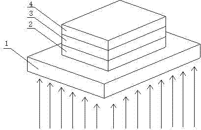
[0029] Embodiment 1: a kind of bottom detection photovoltaic type organic ultraviolet semiconductor detector, with quartz plate as substrate 1, the AZO of 150nm is deposited on substrate 1 with the method for thermal evaporation, forms high work function electrode layer 2; Alkanes and DMF dissolve the fluorene polymer, spin-coat 100nm fluorene polymer on the high work function electrode layer 2 with a homogenizer to form the organic ultraviolet semiconductor layer 3; finally use thermal evaporation technology to deposit 150nm Mg:Ag alloy to form Low work function electrode layer 4 .

Embodiment 2

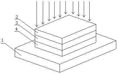
[0030] Embodiment 2: a kind of top detection photovoltaic type organic ultraviolet semiconductor detector, with quartz sheet as substrate 1, the Nb of 150nm is deposited on substrate 1 with magnetron sputtering method to form low work function electrode layer 4, then use heat 100nm fluorene was deposited by evaporation technology to form organic ultraviolet semiconductor layer 3 , and finally 150nm ITO was deposited by magnetron sputtering to form high work function electrode layer 2 .

Embodiment 3

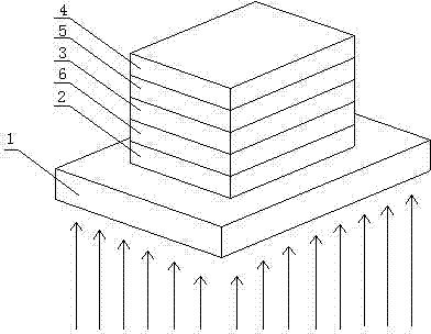
[0031] Embodiment 3: a kind of bottom detection photovoltaic type organic ultraviolet semiconductor detector, with quartz plate as substrate 1, the ITO of 200nm is deposited on substrate 1 with the method for magnetron sputtering, forms high work function electrode layer 2, then Deposit 10nm NPD sequentially by thermal evaporation to form a hole transport layer 6, 100nm phenanthrene, and form an organic ultraviolet semiconductor layer 3, 10nm Alq 3 An electron transport layer 5 is formed, and finally a 150nm Mg:Ag alloy is deposited by thermal evaporation to form a low work function electrode layer 4 .


PUM


Abstract

The invention relates to the technical field of photoelectric, in particular to a photovoltaic organic ultraviolet semiconductor detector. In the photovoltaic organic ultraviolet semiconductor detector, functional layers made of special materials are arranged on a substrate made of a special material to form a three-layer, five-layer or seven-layer structure. Compared with an optical waveguide detector, the photoelectric detector has the advantages of quick response speed, low power consumption, easy array formulation, no need of polarization and the like. In addition, an organic semiconductor material overcomes the defects of an inorganic semiconductor material to ensure that preparation cost is lower and large area and large array can be realized easily, and a photosensing material has controllable resistivity, no need of cooling and flexible processing. Thus, the organic ultraviolet semiconductor detector has important potential application value in military affairs, civil use and certain specific fields.

Description

technical field [0001] The invention relates to the field of optoelectronic technology, in particular to a photovoltaic type organic ultraviolet semiconductor detector. Background technique [0002] Ultraviolet light is a general term for radiation with wavelengths from 10nm to 400nm in the electromagnetic spectrum, which cannot cause people's vision. Ultraviolet detectors are devices used to detect ultraviolet light, and are widely used in military and civilian fields such as environmental monitoring, forest fire prevention, scientific research, and missile warning. [0003] The existing materials used to make ultraviolet detectors mainly include inorganic wide-bandgap semiconductor materials such as ZnO, GaN, and SiC. They are characterized by high preparation temperature, narrow application range, and high price, which limits the development and application of ultraviolet detectors. . Germany's Siemens and the University of Oldenburg have reported visible light-UV detec...

Claims


Application Information

Patent Timeline
Patent Type & Authority Patents(China)
IPC IPC(8): H01L51/42H01L51/44H01L51/46
CPCY02E10/50Y02E10/549
Inventor 姬荣斌唐利斌宋立媛陈雪梅马钰王忆锋庄继胜
Owner KUNMING INST OF PHYSICS
Why Eureka
Try Eureka