Pixel driving circuit of organic light-emitting diode

A technology of pixel drive circuit and light-emitting diode, which is applied to instruments, static indicators, etc., and can solve problems such as different brightness, inconsistent drive current values, and uneven images

Active Publication Date: 2011-03-30
AU OPTRONICS CORP
View PDF4 Cites 29 Cited by
  • Summary
  • Abstract
  • Description
  • Claims
  • Application Information

AI Technical Summary

Problems solved by technology

[0007] However, due to the technical factors of thin film transistors, in the display array 13, the driving transistors in each region are electrically different, that is, the threshold voltage values ​​of the driving transistors are different.
Therefore, when a plurality of display units in different regions receive pixel data having the same voltage, due to differences in the threshold voltages of the driving transistors, the values ​​of the driving currents supplied to the OLEDs in these display units are inconsistent, resulting in The brightness produced by the organic light-emitting diodes when receiving the voltage of the same pixel data is different, thus making the picture displayed by the display panel 10 appear uneven

Method used


Image

  • Pixel driving circuit of organic light-emitting diode
  • Pixel driving circuit of organic light-emitting diode
  • Pixel driving circuit of organic light-emitting diode

Examples


Embodiment Construction

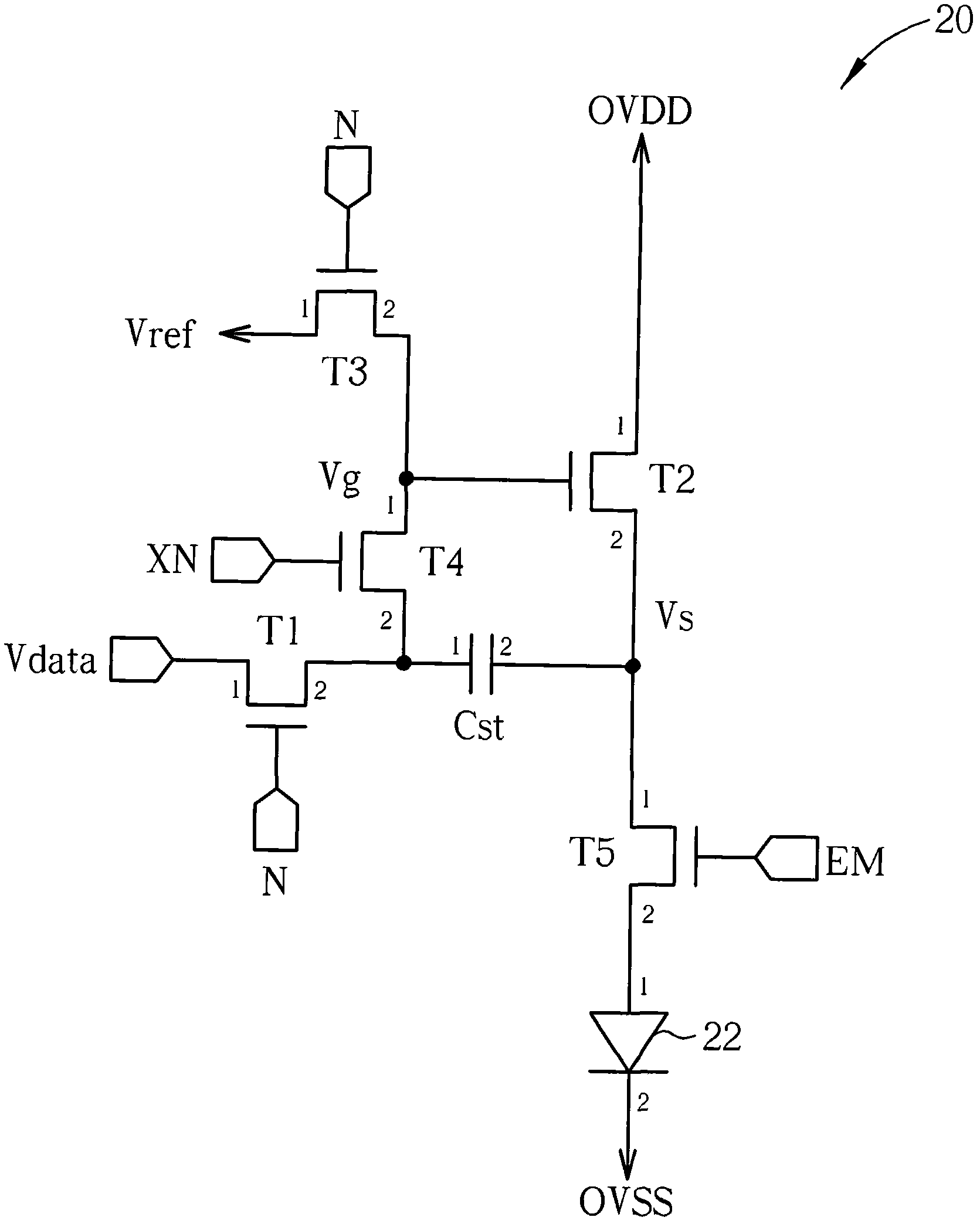
[0029] Please refer to figure 2 , figure 2 It is a schematic diagram of the first embodiment of the pixel driving circuit of the organic light emitting diode of the present invention. The pixel driving circuit 20 includes a first transistor T1, a second transistor T2, a third transistor T3, a fourth transistor T4, a fifth transistor T5, a capacitor Cst, and an organic light emitting diode 22. The first terminal of the first transistor T1 receives the data voltage Vdata, the control terminal of the first transistor T1 receives the first scan signal N, and the second terminal of the first transistor T1 is electrically connected to the first terminal of the capacitor Cst. The first end of the second transistor T2 is electrically connected to the first voltage source OVDD, and the second end of the second transistor T2 is electrically connected to the second end of the capacitor Cst. The first terminal of the third transistor T3 receives the reference voltage Vref, the second ter...


PUM


Abstract

The invention discloses a pixel driving circuit of an organic light-emitting diode, which comprises a first transistor, a capacitor, a second transistor, a third transistor, a fourth transistor, a fifth transistor and an organic light-emitting diode. The operation of the pixel driving circuit mainly comprises three stages, including discharging, data writing, driving lighting. The pixel driving circuit compensates critical voltage of the transistor in the data writing stage so that the driving current of the organic light-emitting diode is unrelated to the change of the critical voltage.

Description

Technical field [0001] The invention relates to a pixel driving circuit of an organic light emitting diode, in particular to a pixel driving circuit of an organic light emitting diode capable of compensating for the critical voltage of a transistor. Background technique [0002] Please refer to figure 1 , figure 1 It is a schematic diagram of a display panel of an organic light emitting diode (OLED) in the prior art. The display panel 10 includes a data driver 11, a scan driver 12 and a display array 13. The data driver 11 controls the data line DL 1 To DL n , And the scan driver 12 controls the scan line SL 1 To SL m . Display array 13 is composed of data line DL 1 To DL n And scan line SL 1 To SL m It is formed by interleaving, and each interleaved data line and scan line forms a display unit, for example, the data line DL 1 And scan line SL 1 The display unit 14 is formed. Such as figure 1 As shown, the equivalent circuit of the display unit 14 (other display units are the s...

Claims


Application Information

Patent Timeline
Patent Type & Authority Applications(China)
IPC IPC(8): G09G3/32G09G3/3233
Inventor 蔡轩名刘俊彦
Owner AU OPTRONICS CORP
Why Eureka
Try Eureka