Supercharge Your Innovation With Domain-Expert AI Agents!

Resistive random access memory and preparation method thereof

A technology of resistive variable memory and thin film, which is applied in the field of memory, can solve the problems of poor transparency and unstable resistance state of resistive variable memory, and achieve the effect of high visible light transparency

Inactive Publication Date: 2011-03-30
INST OF PHYSICS - CHINESE ACAD OF SCI
View PDF0 Cites 7 Cited by
  • Summary
  • Abstract
  • Description
  • Claims
  • Application Information

AI Technical Summary

Problems solved by technology

[0004] However, there are some disadvantages and deficiencies in the resistive memory formed by these materials, mainly because the transparency of such resistive memory is poor, and the resistance state is unstable at high temperature.

Method used


Image

  • Resistive random access memory and preparation method thereof
  • Resistive random access memory and preparation method thereof
  • Resistive random access memory and preparation method thereof

Examples


Embodiment Construction

[0029] The present invention will be described below with reference to specific examples. Those skilled in the art can understand that these examples are only for the purpose of illustrating the present invention, rather than limiting the scope of the present invention.

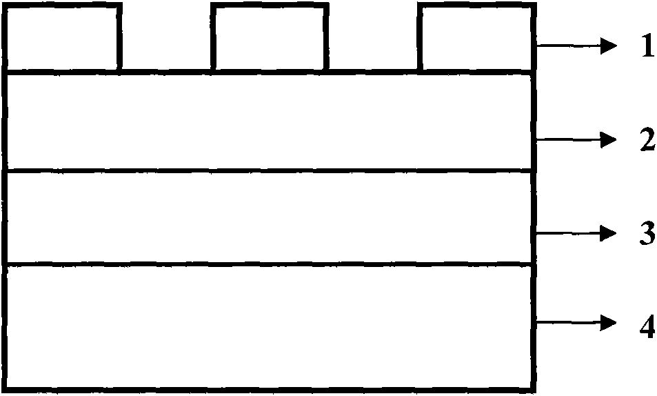
[0030] figure 1 According to an embodiment of the present invention based on WO x Schematic diagram of the structure of a thin-film resistive memory. In the figure, 1 is the top electrode, 2 is WO x Thin film, 3 is the bottom electrode, 4 is the substrate. As shown in the figure, the bottom electrode, WO x The thin film and top electrode are sequentially located above the substrate, WO x The thin film is sandwiched between the bottom and top electrodes, where x ranges from 2≤x≤3. The WO x The film is preferably a single-phase polycrystalline structure and has a thickness of about 10-1000 nm, preferably 300 nm. The thicknesses of the top electrode and the bottom electrode may be, for example, 50-1000 n...


PUM

PropertyMeasurementUnit
Thicknessaaaaaaaaaa

Abstract

The invention provides an electrochromic resistive random access memory and a preparation method thereof. The memory comprises an insulation substrate, a bottom electrode, a WOx film and a top electrode, wherein the bottom electrode is arranged on the insulation substrate, the WOx film is arranged on the bottom electrode, x is in a range greater than or equal to 2 and smaller than or equal to 3, the top electrode is arranged on the WOx film, the insulation substrate can be made of transparent materials, and the bottom electrode and the top electrode can be made of transparent conductive materials. The resistive random access memory according to the invention has the advantages of high transparency, high stability in the wide temperature range at high resistance and low resistance state, nonvolatile storage and the like.

Description

technical field [0001] The present invention relates to the field of memory. Specifically, the present invention relates to a memory with an electro-resistance effect and a preparation method thereof. Background technique [0002] Since the discovery of transparent conductive oxide thin films in the early 20th century, transparent electronic devices have been one of the main directions of optoelectronic technology development. Due to the high transparency of the transparent conductive oxide film in the visible light region, it can be widely used in flat display devices, touch control devices, solar cell devices, photoelectric switching devices, light emitting diodes, electrochromic devices and other fields. Obviously, an ideal transparent electronic device, that is, an electronic device with full transparency, requires that every component of the device has good transparency. At present, by using materials with high transparency and high conductivity, transparency has been...

Claims


Application Information

Patent Timeline
IPC IPC(8): H01L45/00G11C11/56
Inventor 尚大山史磊孙继荣沈保根赵同云
Owner INST OF PHYSICS - CHINESE ACAD OF SCI
Features
  • R&D
  • Intellectual Property
  • Life Sciences
  • Materials
  • Tech Scout
  • Unparalleled Data Quality
  • Higher Quality Content
  • 60% Fewer Hallucinations
Learn More