Driving circuit of pixel and method for driving pixel

A driving circuit and pixel technology, applied in instruments, static indicators, etc., can solve problems such as difference in driving current, uneven brightness of the panel, and afterimage, so as to improve the brightness attenuation, improve the uneven brightness of the panel, and reduce the driving current. the effect of the difference

Inactive Publication Date: 2011-04-06
AU OPTRONICS CORP
View PDF4 Cites 36 Cited by
  • Summary
  • Abstract
  • Description
  • Claims
  • Application Information

AI Technical Summary

Problems solved by technology

Because the brightness of OLEDs is controlled by the driving current, the above-mentioned different driving currents will lead to uneven brightness of the panel
[0003] In addition, due to the influence of the thin film transistor technology, the threshold value (VTH) of the thin film transistor driving each organic light emitting diode is not necessarily the same. Therefore, even if the same data voltage is given, the driving current generated by it will still be different, resulting in panel The brightness is not uniform; in addition, after operating for a period of time, the voltage across the organic light-emitting diode will increase due to the deterioration of the material. Therefore, under the original data voltage operation, the brightness of the pixel will be low, resulting in image sticking The phenomenon

Method used


Image

  • Driving circuit of pixel and method for driving pixel
  • Driving circuit of pixel and method for driving pixel
  • Driving circuit of pixel and method for driving pixel

Examples


Embodiment Construction

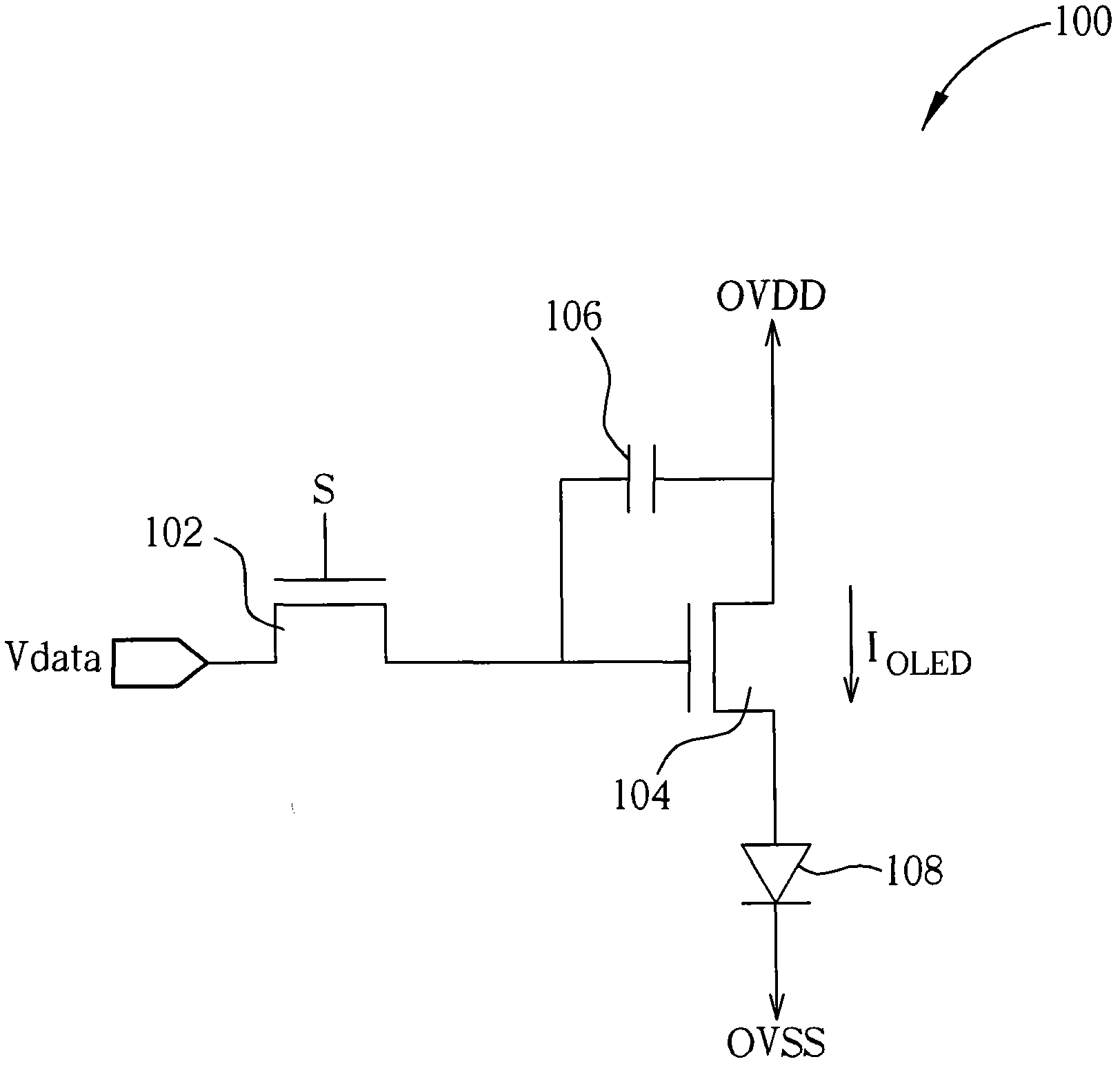
[0035] Please refer to figure 1 , figure 1 It is a schematic diagram illustrating a pixel driving circuit 100 of an active matrix organic light emitting diode (active matrix OLED, AMOLED) display. Such as figure 1 As shown, the driving circuit 100 is a 2T1C circuit, including two N-type thin film transistors 102 , 104 , a capacitor 106 and an organic light emitting diode 108 . The N-type thin film transistor 102 is a switch, and the N-type thin film transistor 104 provides the driving current I of the organic light emitting diode 108. OLED , wherein the OVSS terminals of the driving circuit 100 of each pixel on the panel are electrically connected together, and the OVDD terminals are also electrically connected together. When the driving circuit 100 drives the pixels, there will be a driving current I at the OVSS end. OLED flow past.

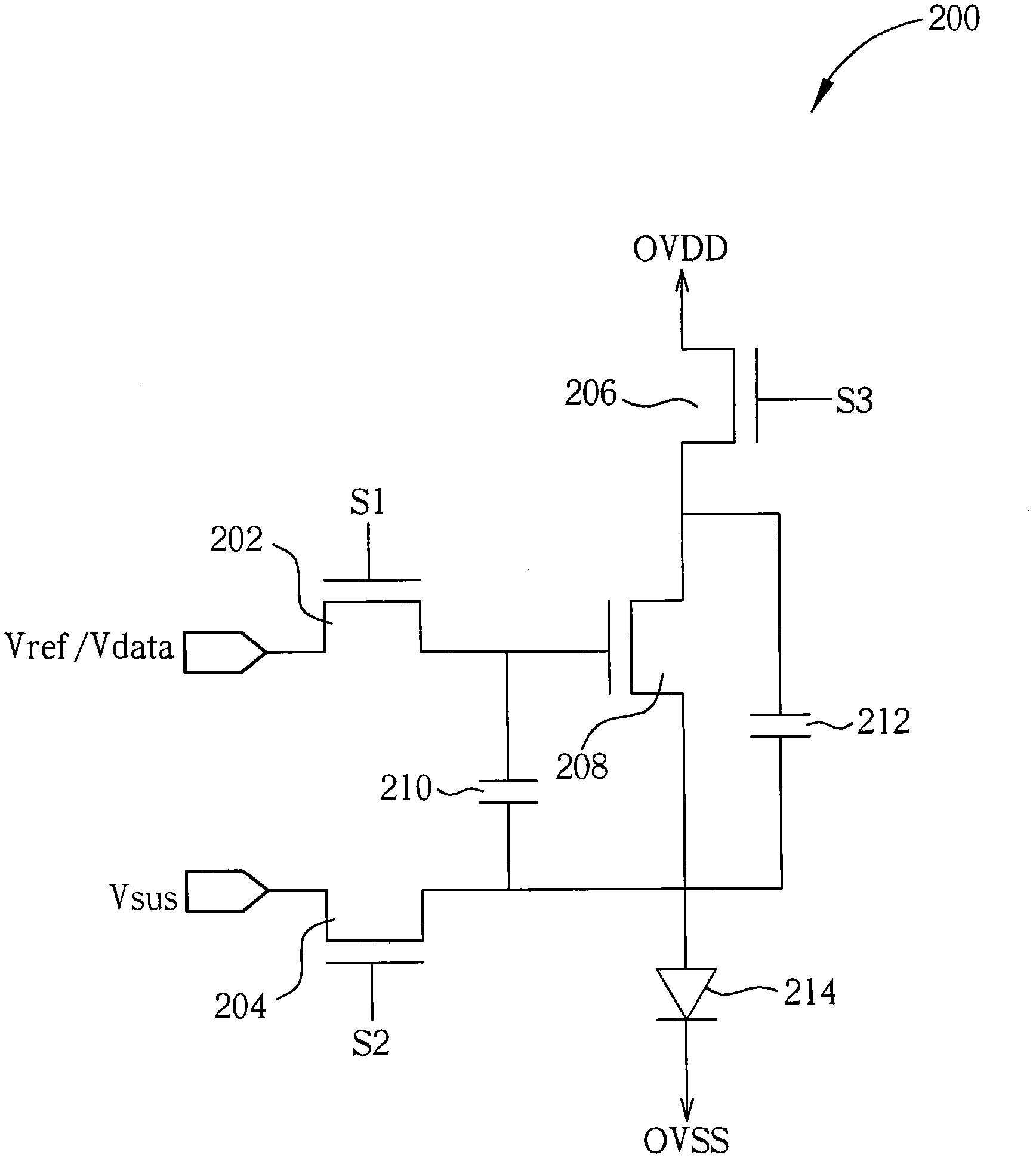
[0036] Please refer to figure 2 , figure 2 A schematic diagram illustrating a pixel driving circuit 200 of an active matrix organic li...


PUM


Abstract

The invention provides a method for driving a pixel and a driving circuit of the pixel. The method comprises the following steps of: charging the first end and the second end of a first capacitor according to a reference voltage and a reset voltage respectively, and simultaneously switching on a third switch; floating the second end of the first capacitor; charging the first end of the first capacitor according to a data voltage, and switching off the third switch; and floating the first end of the first capacitor, and switching on the third switch. Therefore, a driving current irrelevant with the variation of an N-type thin film transistor process and the span voltage of an organic light-emitting diode can be determined by the voltage difference between the first end and the second end of the first capacitor.

Description

technical field [0001] The present invention relates to a driving circuit and a driving method of a pixel of an active matrix organic light emitting diode display, in particular to an active matrix organic light emitting diode display which is not affected by differences in thin film transistor technology and cross-voltage of organic light emitting diodes A pixel driving circuit and a driving method. Background technique [0002] Since the metal line at the common low potential end of the pixel driving circuit of an active matrix organic light emitting diode (active matrix OLED, AMOLED) display has impedance, the source terminals (common low potential end) of the N-type thin film transistors driving different organic light emitting diodes Voltage may vary. In this way, the driving currents flowing through the OLEDs are different. Because the luminance of the OLED is controlled by the driving current, the above-mentioned different driving currents will lead to uneven bright...

Claims


Application Information

Patent Timeline
Patent Type & Authority Applications(China)
IPC IPC(8): G09G3/32G09G3/3225
Inventor 聂建名蔡宗廷
Owner AU OPTRONICS CORP
Why Eureka
Try Eureka