Electric field adjustable negative magnetic conductivity device based on liquid crystal and manufacturing method
A production method and adjustable negative technology, applied in the direction of waveguide devices, electrical components, instruments, etc., can solve the problems of time-consuming and labor-intensive, and achieve the effect of dynamically adjustable working frequency
- Summary
- Abstract
- Description
- Claims
- Application Information
AI Technical Summary
Problems solved by technology
Method used
Image
Examples
Embodiment 1
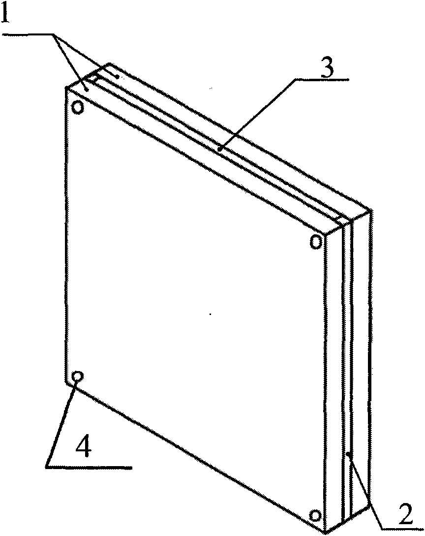
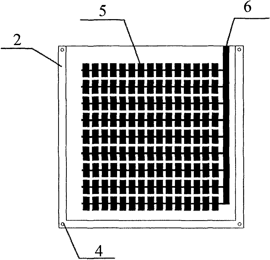
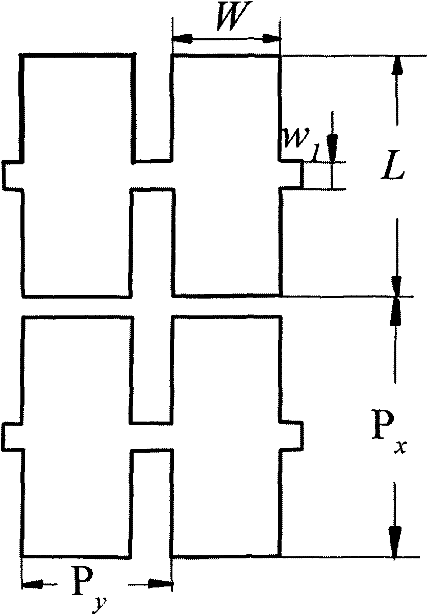
[0041] Embodiment 1: use circuit board printing technology to etch rectangular metal sheet 5 arrays and electrodes 6 on one side of a copper clad laminate 1 with a thickness of 1.00mm, the size of the metal sheet 5 is: W=4.00mm, W 1 =1.00mm, L=9.00mm, Px=11.00mm, Py=6.00mm. Positioning holes 4 with a diameter of 1.00 mm are machined at the four corners of the copper clad laminate 1 . An epoxy glass plate with a thickness of 0.50 mm and the same size as the copper clad laminate 1 is selected, and a U-shaped bead 2 with a side width of 5.00 mm and a positioning hole 4 is prepared by using a numerical control machine tool. Coat the polyimide liquid crystal aligning agent arranged along the surface on the side of the copper-clad laminate 1 with the metal sheet array by the spin coating method, heat-cure the film by step heating method, and use a dust-free cloth on the polyimide film along the Orientation rubbing in the direction of the electrodes to obtain a polyimide liquid crys...
Embodiment 2
[0045] Example 2: A rectangular metal sheet 5 array and electrodes 6 are prepared on a copper clad laminate 1 with a thickness of 1.00mm by using circuit board printing technology. The size of the metal sheet is: W=5.00mm, W 1 = 0.80 mm, L = 9.00 mm, Px = 12.00 mm, Py = 5.00 mm, and at the same time, a positioning hole 4 with a diameter of 1.00 mm is machined at the four corners of the copper clad laminate 1 . Select an epoxy glass plate with a thickness of 0.40 mm and the same size as the copper-clad laminate 1, and use a CNC machine tool to prepare a U-shaped bead 2 with a side width of 5.00 mm, and machine the four corners of the U-shaped bead 2 into a positioning plate with a diameter of 1.00 mm. hole. Coat the polyimide liquid crystal aligning agent arranged along the surface on the side of the copper-clad laminate 1 with the metal sheet array by the spin coating method, heat-cure the film by step heating method, and use a dust-free cloth on the polyimide film along the ...
Embodiment 3
[0048] Example 3: A circular metal sheet 5 array and electrodes 6 were prepared on a copper-clad laminate 1 with a thickness of 1.00 mm by circuit board printing technology, and positioning holes 4 with a diameter of 1.00 mm were machined at the four corners of the copper-clad laminate 1 . The size of circular metal sheet 5 is: R=4.00mm, W 1 =1.00mm, Px=11.00mm, Py=11.00mm. An epoxy glass plate with a thickness of 0.60 mm and the same size as the copper clad laminate 1 is selected, and a U-shaped bead 2 with a side width of 5.00 mm and a positioning hole 4 is prepared by using a numerical control machine tool. Coat the polyimide liquid crystal aligning agent arranged along the surface on the side of the copper-clad laminate 1 with the metal sheet array by the spin coating method, heat-cure the film by step heating method, and use a dust-free cloth on the polyimide film along the Orientation rubbing in the electrode direction to obtain a polyimide liquid crystal alignment laye...
PUM
| Property | Measurement | Unit |
|---|---|---|
| thickness | aaaaa | aaaaa |
| refractive index | aaaaa | aaaaa |
Abstract
Description
Claims
Application Information


