Biface smart card and manufacture method thereof

The technology of a dual-interface smart card and its manufacturing method, which is applied in the field of smart cards, can solve the problems of low production efficiency, high cost, unstable quality of dual-interface smart cards, etc., and achieve the effect of reliable quality, stable quality and low cost

CN102024175AActive Publication Date: 2011-04-20WUHAN TIANYU INFORMATION IND
4 Cites 25 Cited by

Patent Information

Authority / Receiving Office
CN · China
Current Assignee / Owner
Publication Date
2011-04-20

Smart Images

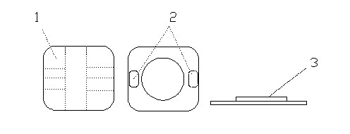
  • Figure 1
    Figure 1
  • Figure 2
    Figure 2
  • Figure 3
    Figure 3
Patent Text Reader

Abstract

The invention discloses a manufacture method of a biface smart card. The manufacture method comprises following steps: 1, punching a conductive bonding pad accommodating hole on a middle sandwich layer (4); 2, loading a conductive bonding pad; 3, embedding wires and welding; 4, piling up and laminating; 5, utilizing a slotter to mill a first-layer groove (8) and a second-layer groove (9) on a clamp body (11) through one step; 6, milling two conductive holes; 7, filling a conducting material (12) into the two conductive holes (10); and 8, finally packaging to form the biface smart card. The biface smart card provided by the invention has the following advantages: the conductive bonding pad is connected with a chip through the conducting material which has more reliable quality and lower cost than those of the existing conductive adhesive; and in addition, an antenna is connected with the conductive bonding pad though a wire embedding machine, such butt-joint process is widely used in contactless cards at present, and the quality is quite stable.
Need to check novelty before this filing date? Find Prior Art

Description

technical field

[0001] The invention relates to the field of smart cards, in particular to a dual-interface smart card and a manufacturing method thereof. Background technique

[0002] The dual-interface smart card is a CPU card that integrates two communication interfaces, contact and non-contact. It combines the advantages of contact and non-contact IC cards, and has the characteristics of large storage capacity, strong reliability, high security, and strong applicability, so it is widely used in finance, telecommunications, public transportation, social insurance and other fields.

[0003] As a new technology, the dual-interface smart card also has its special requirements for card packaging. There are two main packaging processes currently used: conductive adhesive process and butt welding process. Due to the processing technology and conductive rubber problems of the conductive adhesive process, the connection between the antenna and the contact of some cards is unsta...

Examples

Embodiment Construction

[0027] The present invention will be described in further detail below in conjunction with the accompanying drawings and specific embodiments.

[0028] A method for making a dual-interface smart card, comprising the steps of:

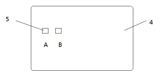
[0029] Step 1: Punch holes for placement of conductive pads. see figure 2 , on the central core layer 4 in the card body 11, two conductive pad placement holes A and B are punched out, and the punching area is located in the position area of ​​a layer of slots 8 to be milled out in the subsequent slot milling process, And avoid the location area of ​​the two-layer groove 9.

[0030] The shape of the hole depends on the shape of the conductive pad. In this embodiment, the two holes are in the shape of a "mouth". The size of the hole is controlled at 2.5*2.5mm. mm, the distance from the upper edge of the card body is 23.9±0.3mm, holes A and B are arranged in parallel, and the distance between the two holes is 11.2±0.3mm.

[0031] Step 2: Fill the con...