Method for improving gluing capacity

A technology of glue coating and glue production, which is applied in the fields of photoplate-making process coating equipment, electrical components, semiconductor/solid-state device manufacturing, etc. The effect of the dead angle problem

Active Publication Date: 2011-04-20
SHENYANG KINGSEMI CO LTD
View PDF2 Cites 3 Cited by
  • Summary
  • Abstract
  • Description
  • Claims
  • Application Information

AI Technical Summary

Problems solved by technology

[0005] The purpose of the present invention is to provide a method for improving the production capacity of glue spraying, so as to solve the problems of low production capacity of silicon wafer spraying in the prior art.

Method used


Image

  • Method for improving gluing capacity
  • Method for improving gluing capacity
  • Method for improving gluing capacity

Examples


Embodiment

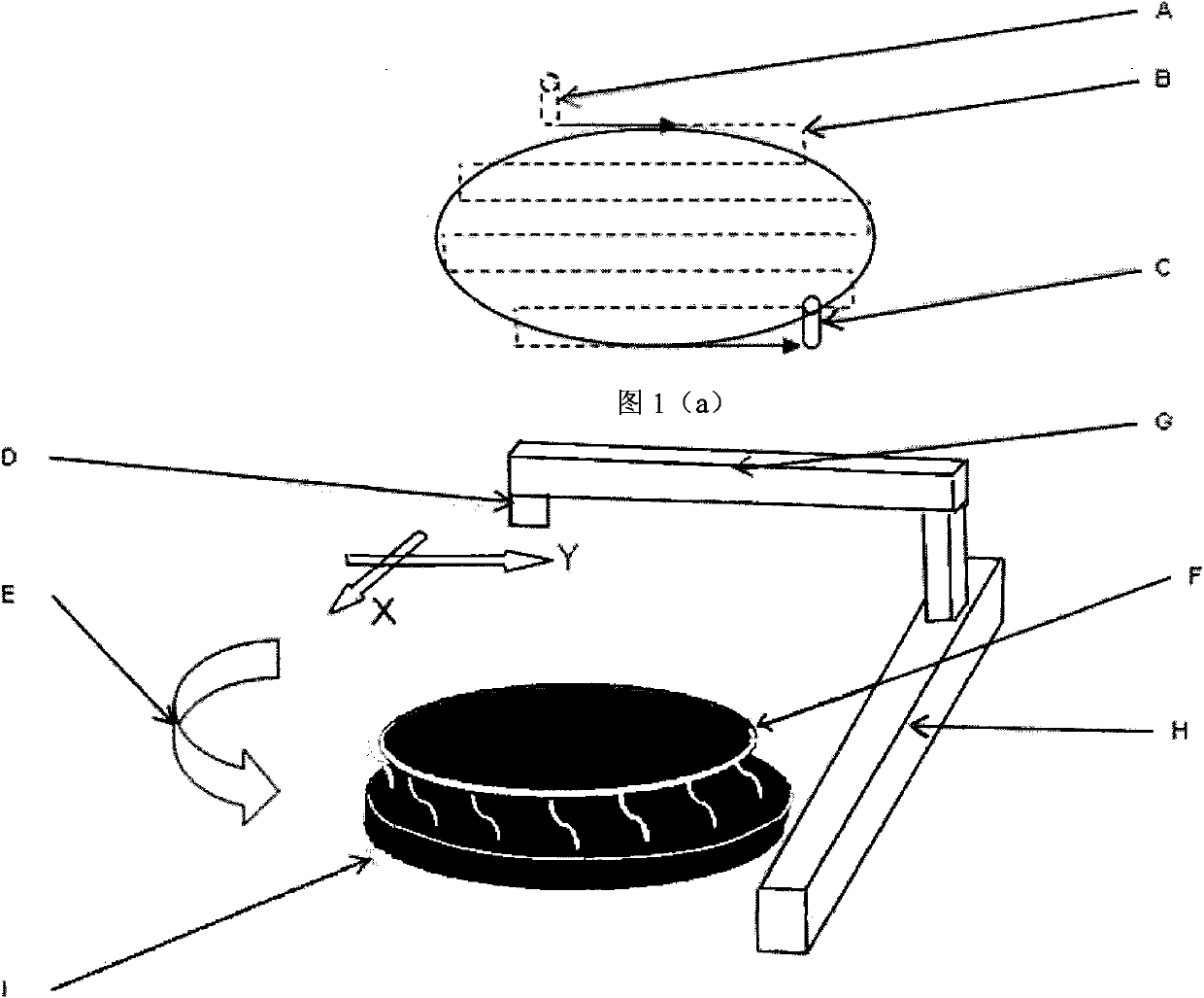
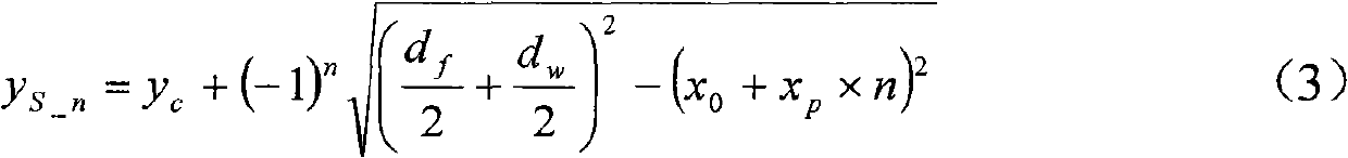
[0042] In this embodiment, the height distance between the spraying glue nozzle and the silicon chip to be coated is 35mm, and the diameter of the silicon chip to be sprayed is d w 200mm (8 inches), the final diameter of the spot circle formed by spraying on the silicon wafer d f =20mm, the coordinates of the center of the silicon wafer (x c ,y c )=(0,0).

[0043] According to formula (1)x 0 =0-(20 / 2+200 / 2)=-110mm, x p = 20mm.

[0044] In this embodiment, when the glue nozzle is at the glue end position, n=11, x n =110,y S_n =0,y O_n =0.

[0045] In the present invention, during the scanning process of the gluing nozzle, the silicon wafer F is still. After one spray coating is completed, the silicon wafer F can be rotated by a certain angle (generally an integer multiple of 90°, 90° in this embodiment) along the rotation direction E of the silicon wafer as required, and then the next spraying is carried out until the photosensitive adhesive is evenly coated On the su...


PUM


Abstract

The invention relates to a silicon wafer processing technique in integrated circuit fabrication, in particular to a method for improving gluing capacity, aiming at solving the problem that capacity of spraying on silicon wafer is low in the prior art. The method is as follows: firstly, a processing carrier silicon wafer is placed on a wafer bearing platform; then a gluing nozzle is used for gluing from an initial position corresponding to one end of silicon wafer, and the gluing nozzle does two-dimensional reciprocating scanning between the initial position and corresponding end position at the other end of the silicon wafer in one plane while spraying photoresist, so that the surface of the silicon wafer is uniformly glued. In the invention, the spray type gluing nozzle is adopted to circuitously reciprocate along X axis and Y axis, the scanning path of the gluing nozzle at the periphery of the silicon wafer is shortened, and the gluing capacity is improved.

Description

technical field [0001] The invention relates to a silicon chip processing technology for integrated circuit manufacturing, in particular to a method for improving the production capacity of gluing. Background technique [0002] The photolithography process in the semiconductor field transfers the pattern on the mask plate to the photoresist coated on the surface of the silicon wafer through exposure, and then transfers the pattern to the wafer through development, etching and other processes. The lithography process directly determines the feature size of semiconductor integrated circuits and is a key technology in the semiconductor field. [0003] In the photolithography process, the photoresist needs to be evenly coated on the silicon wafer before the exposure process is performed. The uniformity of photoresist coating directly affects the yield of photolithography. The commonly used glue coating method uses a column type nozzle. During the coating process, the column typ...

Claims


Application Information

Patent Timeline
Patent Type & Authority Applications(China)
IPC IPC(8): H01L21/027G03F7/16
Inventor 郑春海郑右非汪明波
Owner SHENYANG KINGSEMI CO LTD
Why Eureka
Try Eureka