ESD protective device

An ESD protection and protection device technology, applied in emergency protection circuit devices, circuit devices, emergency protection circuit devices for limiting overcurrent/overvoltage, etc., can solve problems such as poor conduction uniformity, and achieve higher gate voltage. , The effect of reducing the on-voltage and improving the ESD protection capability

Active Publication Date: 2011-04-20
SHANGHAI HUAHONG GRACE SEMICON MFG CORP
View PDF4 Cites 13 Cited by
  • Summary
  • Abstract
  • Description
  • Claims
  • Application Information

AI Technical Summary

Problems solved by technology

[0006] The problem solved by the present invention is to provide an ESD protection device to solve the problem of poor conduction uniformity of the existing ESD protection device

Method used


Image

  • ESD protective device
  • ESD protective device
  • ESD protective device

Examples


no. 1 example

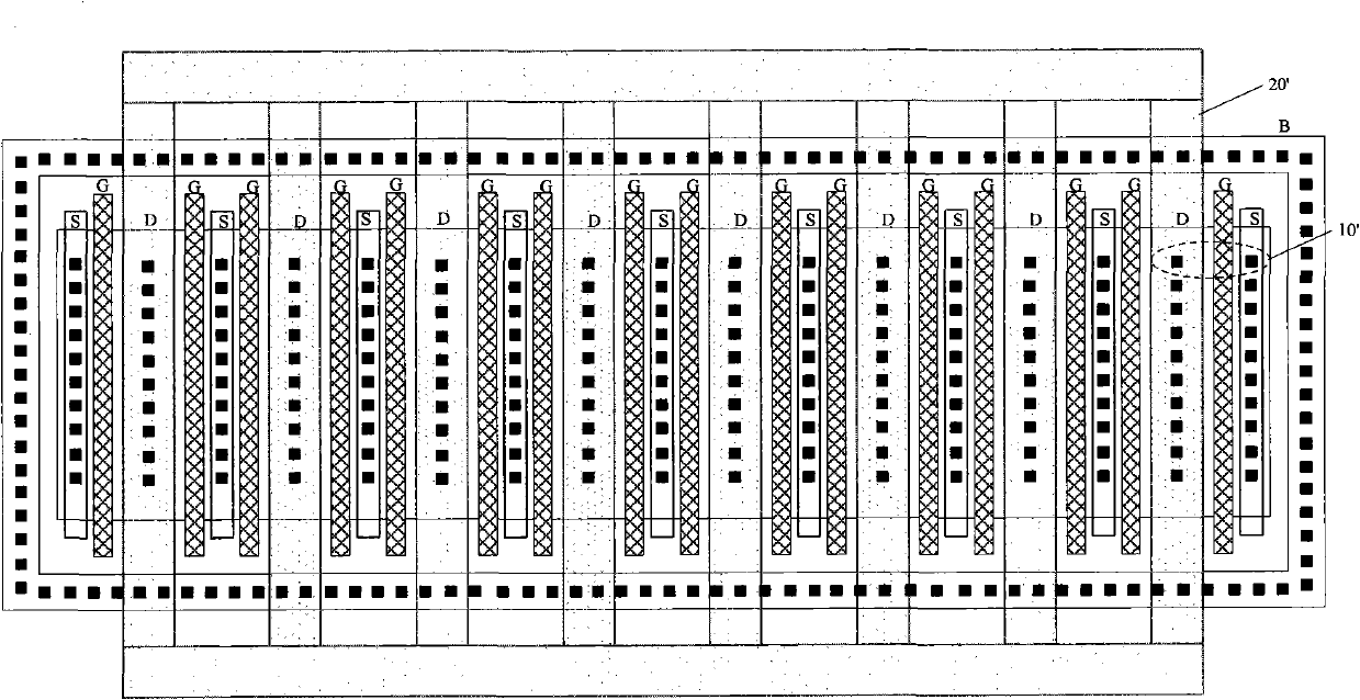
[0032] The ESD protection device provided by this embodiment is as Figure 5 As shown, the device is a multi-finger NMOS protection device located in a P well, and the device includes: a plurality of enhanced NMOS transistors 10 and a multi-finger metal layer 20 .

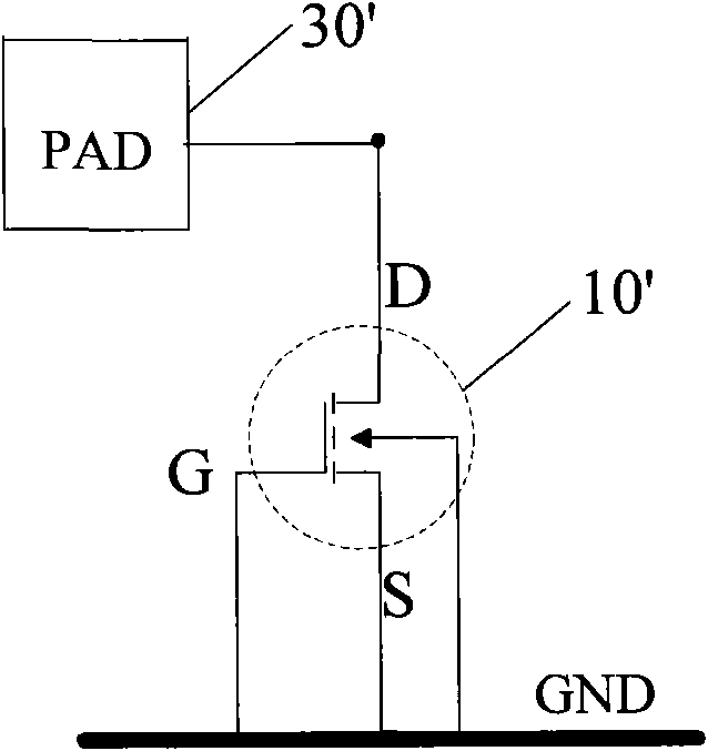
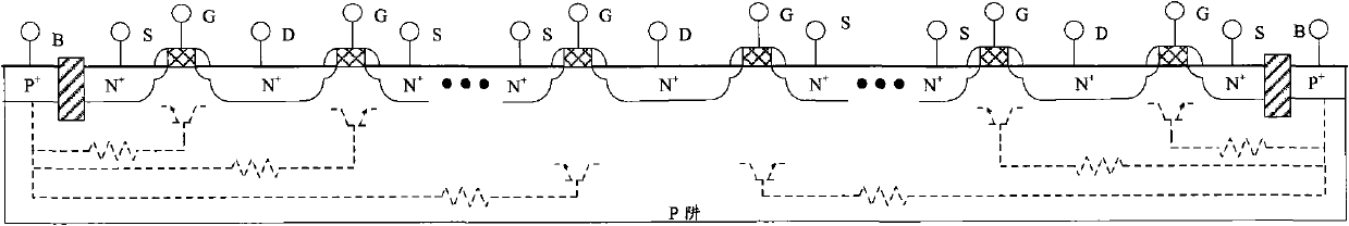
[0033] The plurality of enhanced NMOS transistors 10 are arranged in a matrix, and the cross-sections of the NMOS transistors 10 in each row are shown in Image 6 ; The source S and grid G ​​of the NMOS transistor 10 are grounded (see Figure 7 ); the base of each parasitic NPN transistor of the NMOS transistor 10 is grounded through the parasitic base resistance in the P well. In this embodiment, the base of the parasitic NPN transistor is grounded through the base resistor, specifically, the B that is in contact with the P well is grounded; the black square is a tungsten plug.

[0034] The metal layer 20 covers the drains D of each row of the NMOS transistors 10 and overlaps the gates G of two columns adjacent ...

no. 2 example

[0039] This embodiment provides an ESD protection device (see Figure 5 ), the device is a multi-finger PMOS protection device located in an N well, and the device includes a plurality of enhanced PMOS transistors and a multi-finger metal layer.

[0040] The multiple enhanced PMOS transistors are arranged in a matrix; the source and gate of the PMOS transistors are grounded; the base of each parasitic PNP transistor of the PMOS transistors is grounded through the parasitic base resistance in the N well.

[0041] The metal layer covers the drains of each row of the PMOS transistors and overlaps with the two rows of gates adjacent to the drains, the metal layer is connected to the PAD and connected to the drains; the metal layer is connected to the drains The overlapping gates form parasitic capacitance.

[0042] When a negative ESD pulse occurs on the PAD, the parasitic capacitance couples the gate voltage to a negative potential, increases the leakage current from the drain t...


PUM


Abstract

The present invention relates to an ESD protective device, wherein, the device is a multi-finger MOS protective device, comprising: a plurality of enhanced MOS tubes arranged in matrix. Source electrodes and grid electrodes of the MOS tubes are grounded; the base electrode of the parasitic triode of each MOS tube is grounded through a base electrode resistor; a multi-finger-type metal layer is formed like that the drain electrode of the MOS pipe of each column is covered by the metal layer which is overlapped with two columns of grid electrodes adjacent to the drain electrode, and the metal layer is not only connected with a PAD but also connected with the drain electrode; the parasitic capacitance is produced as the metal layer is overlapped with the grid electrode. For the ESD protective device of the invention, when ESD pulse appears, the parasitic capacitance couples the grid voltage to a nonzero potential so as to produce enough leakage current, so that parasitic triodes of the ESD protective device are simultaneously conducted and discharged. Thus, the conducted voltage is reduced. Besides, the uniformity of conduction is high and ESD protected capability is highly improved.

Description

technical field [0001] The invention relates to the field of protection circuit design of semiconductor integrated circuits, in particular to an ESD protection device. Background technique [0002] During the manufacture, packaging and use of integrated circuit chips, ESD (Electro Static Discharge, electrostatic discharge) phenomenon will occur. ESD is manifested as an instantaneous high-voltage pulse, and the large amount of charge released in this instant is very likely to destroy the functional devices inside the integrated circuit. Therefore, a protection device is usually provided between the internal circuit and the external signal source or power supply. [0003] An existing ESD protection device adopts a multi-finger NMOS design. Such as figure 1 As shown, the outer rectangular frame is covered with Bucks (referred to as B, that is, P well contact, which is generally grounded for NMOS transistors), and each black square represents a through hole of B; each column ...

Claims


Application Information

Patent Timeline
Patent Type & Authority Applications(China)
IPC IPC(8): H02H9/00H02H9/04H01L23/60
Inventor 单毅何军
Owner SHANGHAI HUAHONG GRACE SEMICON MFG CORP
Why Eureka
Try Eureka