Method and device for resource element mapping
A technology of a mapping device and a mapping method, applied in the field of resource mapping, can solve problems such as the inability to meet the high processing capability requirements of the LTE system, and achieve the effects of simplifying logic complexity and high processing capability
- Summary
- Abstract
- Description
- Claims
- Application Information
AI Technical Summary
Problems solved by technology
Method used
Image
Examples
Embodiment Construction
[0032] The technical solutions of the present invention will be further elaborated below in conjunction with the accompanying drawings and specific embodiments.
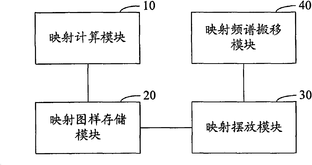
[0033] A resource element mapping device provided by the present invention, such as image 3 As shown, use the hardware description language (HDL, Hardware Description Language) to split the RE mapping into N (N≥2) modules for processing, and each module performs pipeline operations (that is, each module is working at every moment), In order to achieve the purpose of improving system processing capability and simplifying logic complexity.
[0034] image 3 The shown device mainly includes: a mapping calculation module 10 , a mapping pattern storage module 20 and a mapping placement module 30 . The mapping calculation module 10 is used to calculate the signal type that should be placed in each RE of the symbol based on the frame number, subframe number, and symbol number that are two symbols ahead of the system time...
PUM
 Abstract
Description
Claims
Application Information


