Supercharge Your Innovation With Domain-Expert AI Agents!

Liquid crystal display device

A technology of liquid crystal display device and thin film transistor, which is applied in the directions of optics, instruments, electrical components, etc., can solve the problems of decreased display quality and poor screen brightness, and achieve the effect of suppressing the decline of display quality.

Inactive Publication Date: 2013-03-20
CASIO COMPUTER CO LTD
View PDF2 Cites 0 Cited by
  • Summary
  • Abstract
  • Description
  • Claims
  • Application Information

AI Technical Summary

Problems solved by technology

Therefore, even when voltages corresponding to mutually equal grayscale levels are written into the respective pixel electrodes, the voltages held in the pixel electrodes are different for each row. In the case of the screen, there will also be a difference in brightness within the screen, and there will be a problem that the display quality will deteriorate.

Method used


Image

  • Liquid crystal display device
  • Liquid crystal display device
  • Liquid crystal display device

Examples


Embodiment Construction

[0055] Embodiments of the present invention will be described below.

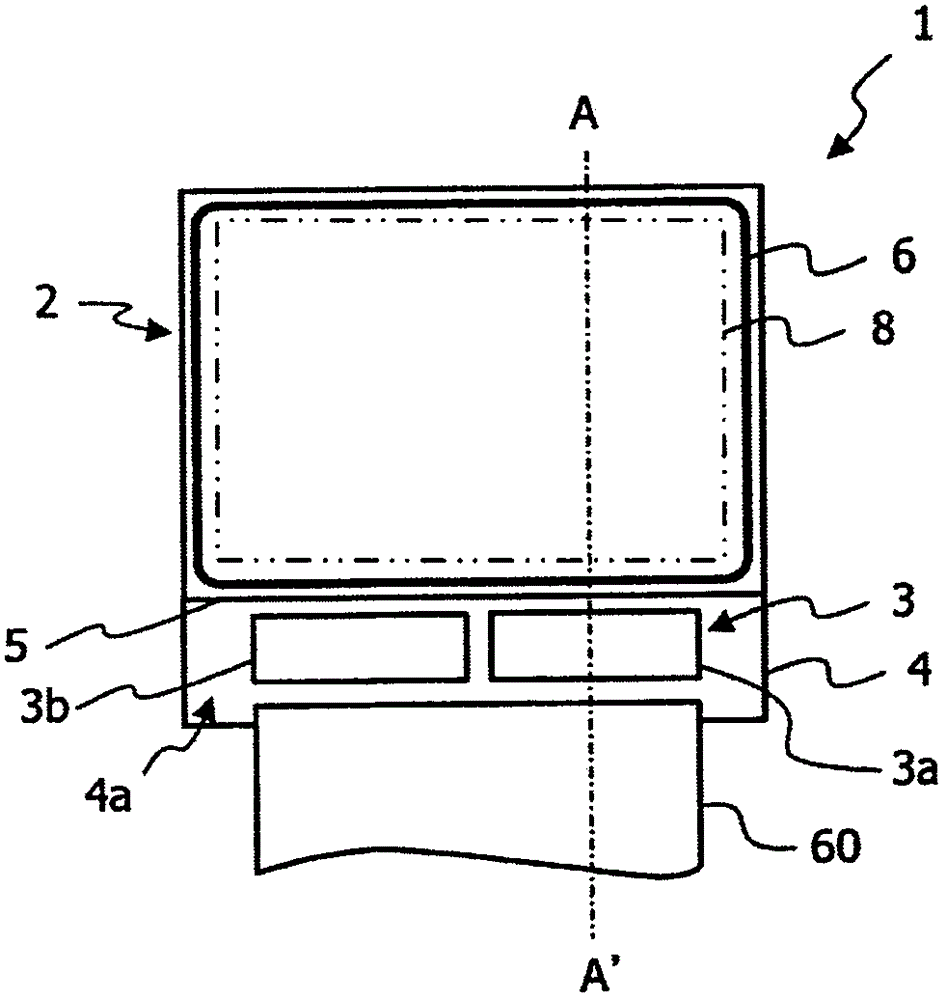
[0056] As the liquid crystal display device of the present invention, in figure 1 A schematic plan view of an active-matrix liquid crystal display device is shown in figure 2 Indicates its cross-sectional view. The liquid crystal display device 1 includes a display panel 2 , a driver circuit 3 for driving the display panel 2 , and FPC (Flexible printed circuits) 60 for connecting the driver circuit 3 to an external circuit. The driver circuit 3 is composed of a gate driver 3a and a data driver 3b. Furthermore, the gate driver 3 a and the data driver 3 b are respectively constituted by IC chips as semiconductor elements, are mounted on the display panel 2 by COG (Chip on Glass) mounting in a predetermined area of ​​the display panel 2 .

[0057] In the display panel 2 , an active substrate 4 is bonded to a counter substrate 5 arranged to face the active substrate 4 via a substantially square frame-shaped...


PUM


Abstract

A display apparatus includes a first gate line extended in a predetermined direction; a second gate line extended in parallel to the first gate line; a first gate output terminal corresponding to the first gate line; a second gate output terminal corresponding to the second gate line; a first gate leading line electrically connecting the first gate line to the first gate output terminal; a second gate leading line electrically connecting the second gate line to the second gate output terminal and having a length longer than said first gate leading line; and a static electric protection line disposed so as to overlap the first gate leading line and the second gate leading line with an insulating layer interposed between said static electric protection line and the first and second gate leading lines, wherein an overlapping area between the first gate leading line and the static electric protection line is larger than an overlapping area between the second gate leading line and the static electric protection line.

Description

technical field [0001] The present invention relates to a liquid crystal display device in which a wiring length of a connection wiring electrically connecting a gate line for transmitting a scan signal to a thin film transistor and a predetermined connection terminal is different for each gate line. Background technique [0002] As a liquid crystal display device, an active matrix liquid crystal display device includes a thin film transistor (Thin Film Transistor: hereinafter referred to as TFT) and a pixel electrode connected to the TFT near the intersection of gate lines and source lines. [0003] In addition, a liquid crystal layer is formed between the pixel electrode and a counter electrode (common electrode) arranged to face the pixel electrode. [0004] And, by applying a voltage corresponding to the grayscale level to the pixel electrode through the TFT selected by the scanning signal input through the gate line, the alignment state of the liquid crystal is changed ...

Claims


Application Information

Patent Timeline
Patent Type & Authority Patents(China)
IPC IPC(8): G02F1/1362G02F1/1368H01L27/12
CPCG02F2001/13456H01L27/1214G02F2202/22H01L27/12G02F1/1345H01L27/124G02F1/13456
Inventor 渡边仁石井裕满
Owner CASIO COMPUTER CO LTD
Features
  • R&D
  • Intellectual Property
  • Life Sciences
  • Materials
  • Tech Scout
  • Unparalleled Data Quality
  • Higher Quality Content
  • 60% Fewer Hallucinations
Learn More