ESD (Electrostatic Discharge) protective circuit

An electrostatic discharge protection and circuit technology, applied in emergency protection circuit devices, emergency protection circuit devices for limiting overcurrent/overvoltage, circuits, etc., can solve problems such as inability to provide ESD protection for internal circuits, and achieve low trigger voltage , strong protective effect

Active Publication Date: 2011-04-27
STATE GRID CORP OF CHINA +2
View PDF0 Cites 4 Cited by
  • Summary
  • Abstract
  • Description
  • Claims
  • Application Information

AI Technical Summary

Problems solved by technology

[0009] To sum up, the trigger voltage of SCR depends on the voltage applied to the anode when the PN junction composed of PWELL and NWELL undergoes reverse breakdown. This voltage needs to be very high and cannot provide effective ESD protection for the internal circuit.

Method used


Image

  • ESD (Electrostatic Discharge) protective circuit
  • ESD (Electrostatic Discharge) protective circuit
  • ESD (Electrostatic Discharge) protective circuit

Examples


Embodiment Construction

[0021] In order to make the above objects, features and advantages of the present invention more comprehensible, specific implementations of the present invention will be described in detail below in conjunction with the accompanying drawings.

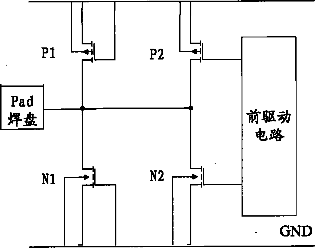
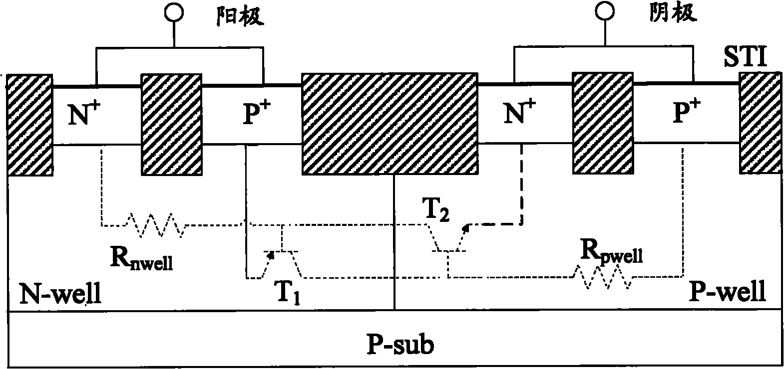
[0022] An electrostatic discharge protection circuit provided by an embodiment of the present invention includes a PMOS transistor, an NMOS transistor and an SCR transistor. Specifically: set N-well contacts around the PMOS tube, set P-well contacts around the NMOS tube, insert a P+ and a N+ between the N-well contact and the P-well contact in sequence, and the N -well contact, one P+, ​​one N+ and P-well contact form at least two SCR tubes.

[0023] see image 3 , which is the layout of the ESD protection circuit of the present invention.

[0024] The ESD protection circuit provided by the embodiment of the present invention includes a PMOS transistor, an NMOS transistor and an SCR transistor.

[0025] From image 3 As can be seen...


PUM


Abstract

The invention relates to an ESD (Electrostatic Discharge) protective circuit, which comprises an N-well contact arranged around a PMOS (P-channel Metal Oxide Semiconductor) tube and a P-well contact arranged around an NMOS (N-channel Metal Oxide Semiconductor) tube. A P+ and an N+ are inserted respectively between the N-well and P-well contacts. The N-well contact, P+, N+ and P-well contact form an SCR tube. The ESD protective capacity in unit size of the SCR is greater than that of the MOS tube. The reverse breakdown voltage of a grid diode at the junction of a drain and a grid of the NMOS tube of the circuit is lower so the drain with ESD impulse can generate drain current by means of reverse breakdown under lower voltage so that the base-emitter of a T2 of the SCR is positively biased, the T2 is conducted and finally the whole SCR structure is conducted. The triggering voltage of the ESD protective circuit is low and the protective capacity is far stronger than that of the single MOS tube once the SCR can be triggered and conducted.

Description

technical field [0001] The invention relates to the technical field of electrostatic discharge protection, and particularly designs an electrostatic discharge protection circuit. Background technique [0002] see figure 1 , which is a structure diagram of an output driving circuit and an electrostatic discharge (ESD, Electro Static Discharge) protection circuit of an input and output unit in the prior art. [0003] P1 and P2 are PMOS tubes, and N1 and N2 are NMOS tubes. The circuit composed of P1 and N1 can be used not only as an ESD protection circuit, but also as an output drive circuit of the input and output unit, from figure 1 It can be seen that the circuit composed of P1 and N1 on the left is used as an ESD protection circuit. The circuit composed of P2 and N2 on the right is the output drive circuit as the input and output unit. [0004] The only difference between the ESD protection circuit and the output drive circuit of the I / O unit is the position of the gate...

Claims


Application Information

Patent Timeline
Patent Type & Authority Applications(China)
IPC IPC(8): H01L27/02H01L23/60H02H9/00
Inventor 单毅
Owner STATE GRID CORP OF CHINA
Why Eureka
Try Eureka