Method for processing high-precision PCB (Printed Circuit Board) with nonmetal and metal edges

A technology of PCB board and processing method, which is applied in the processing field of high-precision non-metallic and metallized PCB boards, can solve the problems of insufficient precision, unfavorable assembly, manual repair, etc., and achieve the effect of high precision

Inactive Publication Date: 2012-10-03
SHENNAN CIRCUITS
View PDF0 Cites 0 Cited by
  • Summary
  • Abstract
  • Description
  • Claims
  • Application Information

AI Technical Summary

Problems solved by technology

[0004] 1. The accuracy is not enough, and the edge of the PCB board whose contact between the metal part and the non-metal part is less than 0.05mm cannot be processed;
[0005] 2. When the existing process is dealing with non-metallic parts, it is easy to produce obvious protrusions, which is not beautiful and unfavorable for final assembly;
[0006] 3. A large number of burrs are generated during mechanical cutting, which requires manual repair, which is time-consuming and laborious

Method used


Image

  • Method for processing high-precision PCB (Printed Circuit Board) with nonmetal and metal edges
  • Method for processing high-precision PCB (Printed Circuit Board) with nonmetal and metal edges
  • Method for processing high-precision PCB (Printed Circuit Board) with nonmetal and metal edges

Examples


Embodiment Construction

[0033] In order to describe the technical content, structural features, achieved goals and effects of the present invention in detail, the following will be described in detail in conjunction with the embodiments and accompanying drawings.

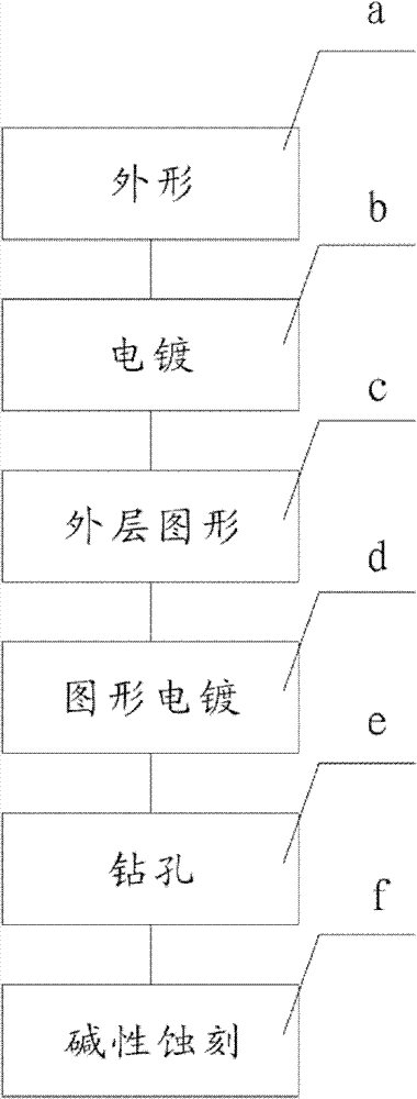
[0034] see figure 1 , the processing method of the high-precision non-metallic PCB board of the present invention, may further comprise the steps:

[0035] a. Shape: directly mill out the shape of the PCB board with a milling machine;

[0036] b. Electroplating: Electroplate a layer of copper on the surface of the PCB board obtained in step a and the non-metallic and metallized edges;

[0037] c. Outer layer graphics: the copper-plated PCB surface obtained in step b needs to be etched to cover the area where the copper is removed;

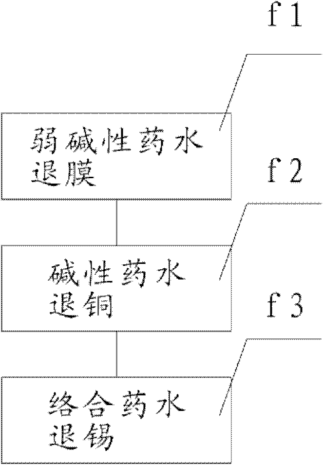
[0038] d. Pattern electroplating: After step c, plate a layer of tin that plays a protective role in etching on the metal area of ​​the PCB surface that is not covered with the dry film and the non-metallic ...


PUM


Abstract

The invention discloses a method for processing a high-precision PCB (Printed Circuit Board) with nonmetal and metal edges. The method comprises the following steps of: (a) determining an external form; (b) electroplating; (c) determining an outer-layer pattern; (d) electroplating the pattern; (3) drilling; and (f) alkaline etching; The method has the advantages that a wet process and a machiningprocess are combined, an board edge of which a contact step is smaller than 0.05mm between the metal part and the nonmetal part of the PCB can be processed, and the precision is high.

Description

technical field [0001] The invention relates to the field of PCB board preparation, in particular to a method for processing a high-precision non-metallic PCB board with metallized edges. Background technique [0002] At present, the processing method of the metal part of the conventional non-metal plus metal edge PCB board is as follows: firstly, the metal part is milled with a CNC milling machine before electroplating, and then metallized by electroplating. The processing method of the non-metal part of the non-metal plus metal edge PCB board is: use a CNC milling machine to mill out the non-metal part, see Figure 9 shown. [0003] The existing non-metallic and metallized edge PCB processing methods have the following disadvantages: [0004] 1. The accuracy is not enough, and the edge of the PCB board whose contact between the metal part and the non-metal part is less than 0.05mm cannot be processed; [0005] 2. When the existing process is dealing with non-metallic par...

Claims


Application Information

Patent Timeline
Patent Type & Authority Patents(China)
IPC IPC(8): H05K3/00
Inventor 丁大舟崔荣
Owner SHENNAN CIRCUITS
Why Eureka
Try Eureka