Micron-nano thermal detecting and sensing component

A sensing component, micro-nano technology, applied in the field of instrument development, can solve problems such as structural incompatibility, and achieve the effect of improving the effective component and enhancing the detection sensitivity

Inactive Publication Date: 2011-05-11
SHANGHAI INST OF CERAMIC CHEM & TECH CHINESE ACAD OF SCI
View PDF0 Cites 11 Cited by
  • Summary
  • Abstract
  • Description
  • Claims
  • Application Information

AI Technical Summary

Problems solved by technology

However, due to technical problems such as the selected test method and the matching of related devices, the resolution of the thermal detection imaging of this commercial product is only 100 nanometers, which is still far from the actual requirements of current nano-scientific research.
At the same time, the thermal detection accessories related to this product are dedicated and structurally incompatible with other commercial AFM instruments, ma...

Method used


Image

  • Micron-nano thermal detecting and sensing component
  • Micron-nano thermal detecting and sensing component
  • Micron-nano thermal detecting and sensing component

Examples


Embodiment 1

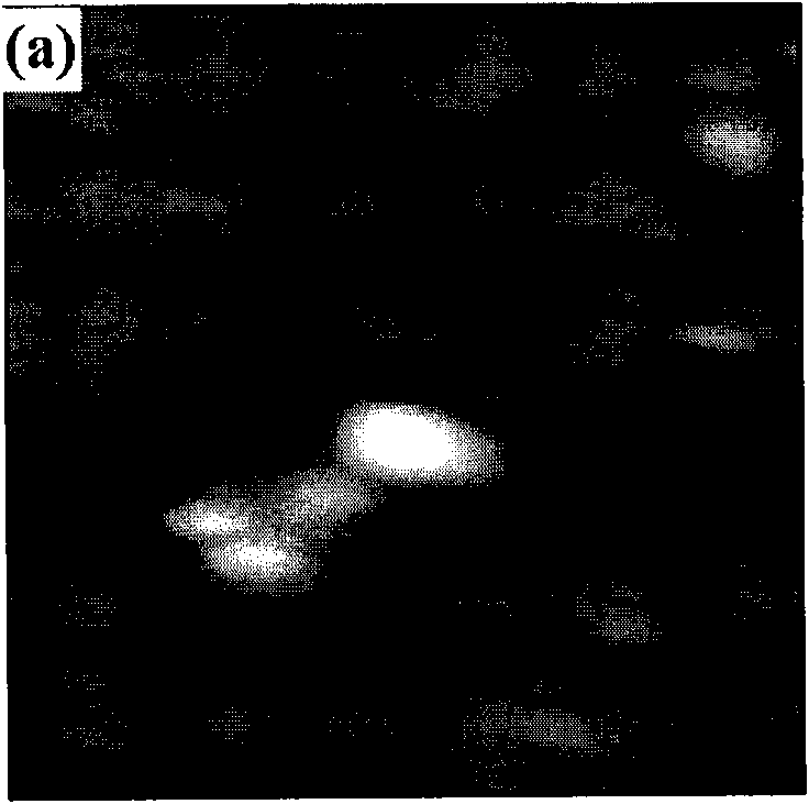
[0029] Embodiment 1: Applying the present invention to carry out thermal detection imaging on low temperature co-fired ceramics (Low Temperature Co-fired Ceramics, LTCC). LTCC is a new electronic packaging material used to achieve high integration and high performance. The devices made are widely used in the fields of high-frequency wireless communication, aerospace industry, and computers. Due to the miniaturization and high integration of devices, the thermophysical properties of their microstructures are closely related to the reliability and service life of devices. So far, there have been no reports on the detection of microscopic thermophysical properties of such materials. Figure 2 shows the test results. Among them, the picture (a) is the topographic AFM image of the sample, which is the original function of the atomic force microscope. The picture (b) is the SThM thermal image reflecting the microscopic thermal physical properties of the sample in situ by the built-u...

Embodiment 2

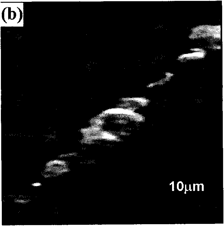
[0031] Embodiment 2: application of the present invention to ferromagnetic memory alloy Ni 53 mn 24 Ga 23 The material was thermally detected and imaged. Figure 3 shows the test results of the topographic and thermal images of the ferromagnetic alloy in the scanning range of 80 μm × 80 μm. Figure 3(a) is a topographical image, showing scratches and defects on the surface, without other information. The thermal image of Figure 3(b) shows a curved microstructure with alternating bright and dark contrasts (as indicated by the arrow). The thermal image of this structure can roughly confirm that the width of these stripes is 3-4 μm. According to the contrast mechanism of scanning thermal imaging, if the influence of the topographic image is excluded, the thermal image mainly reflects the thermal conductivity distribution of the micro-region of the sample. Figure 2 reflects the inhomogeneity of thermal conductivity in ferromagnetic alloy micro-regions, which has not been reporte...


PUM


Abstract

The invention discloses a micron-nano thermal detecting and sensing component, comprising a thermal probe for heating and sensing the temperature of a tested sample, a reference probe for detecting an ambient temperature when the thermal probe is used for detecting, a magnetic base used for gripping the baseboard of the thermal probe by a magnetic force and locating the thermal probe, an isolated body arranged below the magnetic base, a locator which is of a pressing board structure and used for pressing the lead of the thermal probe to assist in locating the thermal probe, an output connection body circuit board and a testing support, wherein the output connection body circuit board comprises a printed circuit board and a connector, the printed circuit board is connected with the output end of the reference probe and the output end of the thermal probe, the connector is used for the connection with an external detecting bridge circuit, and the testing support is used for fixing the output connection body circuit board, the magnetic base, the isolated body and the locator. The component provided by the invention has the characteristics of high detecting sensitivity, strong external environment disturbance resistance and the like, and is completely compatible with a commercial atomic force microscope (AFM) to achieve the in-situ acquisition of the topography image and thermal image of the tested sample. The component provided by the invention has the thermal imaging resolution ratio of 60 nanometers which is better than those of the similar imports.

Description

technical field [0001] The invention relates to a micro-nano thermal detection sensing component, which is a core component in a scanning probe thermal microscopic imaging system and belongs to the field of instrument development. Background technique [0002] With the in-depth development of current nanotechnology, there is an urgent need to develop in-situ, non-destructive, high-resolution detection technologies that can characterize the properties of materials and devices at the micro-nano scale, especially the characterization technology of thermal physical properties. At the micro-nano scale, due to factors such as quantum effects, material limitations, and interface effects, thermophysical properties will produce obvious size effects, which directly affect the performance stability, reliability, and service life of materials and devices. Therefore, how to accurately detect thermal properties at the micro-nano scale has attracted increasing attention. Atomic force micr...

Claims


Application Information

Patent Timeline
IPC IPC(8): G01Q60/24G01Q60/38G01N25/00G01N25/20
Inventor 曾华荣殷庆瑞惠森兴赵坤宇李国荣
Owner SHANGHAI INST OF CERAMIC CHEM & TECH CHINESE ACAD OF SCI
Why Eureka
Try Eureka