Passivation layer dry etching method

A dry etching and passivation layer technology, which is applied in the fields of electrical components, semiconductor/solid-state device manufacturing, circuits, etc., can solve the problems of increased leakage current of gate oxide layer, damage of gate oxide layer, increase of turn-on voltage and current, etc. , to achieve the effect of reducing PID and reducing physical bombardment

Active Publication Date: 2012-05-30
SEMICON MFG INT (SHANGHAI) CORP
View PDF0 Cites 0 Cited by
  • Summary
  • Abstract
  • Description
  • Claims
  • Application Information

AI Technical Summary

Problems solved by technology

The second passivation layer etching is considered to be the root cause of the PID phenomenon, because the plasma will act on the aluminum pad during the second passivation layer etching process, and will be transmitted to the gate oxide through the copper interconnection line in the front layer of the aluminum pad. layer, causing damage to the gate oxide layer, which increases the leakage current of the gate oxide layer
The disadvantage of the former is: the reduction of plasma energy will reduce the etching uniformity of the entire silicon wafer
The disadvantage of the latter is that although increasing the thickness of the gate oxide layer of the source and drain will increase the protection of the source and drain, the increase in the thickness of the gate oxide layer will increase the turn-on voltage and current, making normal operation Does not work properly under voltage

Method used


Image

  • Passivation layer dry etching method
  • Passivation layer dry etching method
  • Passivation layer dry etching method

Examples


Embodiment Construction

[0043] The present invention will be further described in detail below in conjunction with the accompanying drawings and specific embodiments.

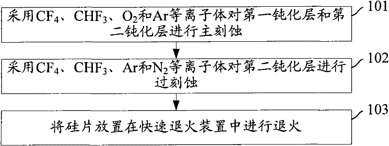
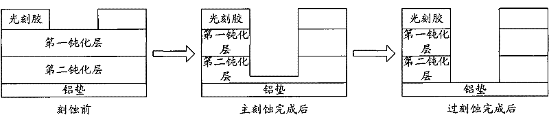
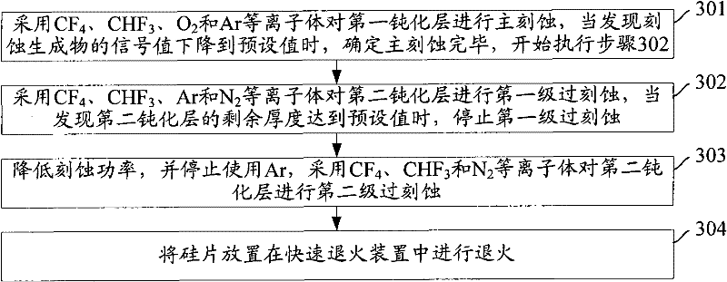
[0044] image 3 The flow chart of the passivation layer dry etching method provided by the embodiment of the present invention, in this embodiment, the first and second passivation layers are located above the aluminum pad, and the second passivation layer is located below the first passivation layer, as shown in image 3 As shown, the specific steps are as follows:

[0045] Step 301: Adopt CF 4 、CHF 3 , O 2 Perform main etching on the first passivation layer with Ar plasma, and when it is found that the signal value of the etching product drops to a preset value, it is determined that the main etching is completed, and step 302 is started.

[0046] Among them, the pressure of the etching chamber is usually: 15-250mt, the etching power is usually: 500-3500w, CF 4The flow rate is usually: 20-300sccm, CHF 3 The flow rate is usuall...


PUM


Abstract

The invention discloses a passivation layer dry etching method. The method comprises the following steps: depositing a second passivation layer and a first passivation layer above an aluminum gasket at the surface of a silicon wafer, wherein the second passivation layer is positioned below the first passivation layer; etching the first passivation layer and the second passivation layer through plasma containing argon Ar; and stopping using Ar and continuing to etching the second passivation layer when the thickness of the second passivation layer is reduced to a pre-set thickness. Through theinvention, the PID is reduced.

Description

technical field [0001] The invention relates to the technical field of semiconductor manufacturing, in particular to a passivation layer dry etching method. Background technique [0002] Etching refers to the selective removal of interconnection materials deposited on the surface of silicon wafers to form circuit patterns generated by photolithography. There are two types of etching processes: dry etching and wet etching. Dry etching is the plasma generated by exposing the surface of the silicon wafer to the gaseous state. The plasma passes through the window opened in the photoresist and reacts physically and / or chemically with the silicon wafer, thereby removing the exposed surface material. [0003] In the metallization process of semiconductor manufacturing, in order to increase the corrosion resistance of interconnect metals such as aluminum, two passivation layers are usually added above the aluminum pad, called the first passivation layer and the second passivation l...

Claims


Application Information

Patent Timeline
Patent Type & Authority Patents(China)
IPC IPC(8): H01L21/311
Inventor 孙武王新鹏
Owner SEMICON MFG INT (SHANGHAI) CORP
Why Eureka
Try Eureka